


Отчет
1. Структурная схема IP ядра UART
Рис. 1.1 Структурная схема IP ядра UART
2. Описание работы модуля
Назначение. IP ядро UART предназначено для организации внешнего интерфейса обмена данными между внешним цифровым устройством и софт-процессором Microblaze по универсальной шине AXI с поддержкой интерфейса AXI4-Lite.
Характеристики:
- данные передаются последовательно по одному байту в сопровождении так называемых «стартового» и «стопового» битов (см. рис. 2.1) по двум независимым линиям rxd и txd приемника и передатчика модуля соответственно; в состоянии ожидания на линиях rxd и txd установлен логический уровень «0»;
Рис. 2.1 Временная диаграмма обмена данными между внешним цифровым устройством и модулем интерфейса UART по независимым линиям rxd и txd
- поддерживаются следующие скорости обмена данными межу софт-процессором Microblaze и внешним цифровым устройством:
ü 9600 бод/сек;
ü 19200 бод/сек;
ü 115200 бод/сек;
- поддержка универсального интерфейса AXI4-Lite;
- IP ядро UART – slave-устройство на шине AXI.
Сигналы модуля и их назначение
Табл. 1 Сигналы IP ядра UART и их назначение
| Имя сигнала | Направление сигнала | Разрядность | Описание |
| S_AXI_ACLK | input | Глобальная тактовая частота, по переднему фронту S_AXI_ACLK синхронизируются все сигналы | |
| S_AXI_ARSTN | input | Глобальный сигнал сброса. Активный уровень – логический «0» | |
| S_AXI_AWADDR | input | Адрес (Memory Mapped) для записи данных в модуль IP ядра UART со стороны Master-устройства на шине AXI (процессора Microblaze) | |
| S_AXI_AWVALID | input | Сигнал подтверждения адреса S_AXI_AWADDR | |
| S_AXI_WDATA | input | Данные для записи в модуль IP ядра UART, выставленные Master-устройством на шине AXI | |
| S_AXI_WSTRB | input | Строб записи данных | |
| S_AXI_WVALID | input | Сигнал подтверждения данных для записи S_AXI_WDATA и строба записи данных S_AXI_WSTRB на шине | |
| S_AXI_BREADY | input | Сигнал готовности Master-устройства на шине AXI принимать ответную информацию | |
| S_AXI_ARADDR | input | Адрес (Memory Mapped) для чтения данных из модуля IP ядра UART со стороны Master-устройства на шине AXI (процессора Microblaze) | |
| S_AXI_ARVALID | input | Сигнал подтверждения адреса S_AXI_ARADDR | |
| S_AXI_RREADY | input | Сигнал готовности чтения данных или ответной информации Master-устройством на шине AXI | |
| S_AXI_ARREADY | output | Сигнал готовности адреса чтения. Указывает на то, что устройство модуля IP ядра UART (slave-устройство на шине AXI) готово принять адрес для чтения и сопровождающие управляющие сигналы | |
| S_AXI_RDATA | output | Данные для чтения из модуля IP ядра UART Master-устройством на шине AXI | |
| S_AXI_RRESP | output | Сигнал статуса операций чтения (известно 4 состояния сигнала S_AXI_RRESP: OKAY, EXOKAY, SLVERR, DECERR) | |
| S_AXI_RVALID | output | Сигнал подтверждения данных для чтения S_AXI_RDATA на шине AXI Master-устройством | |
| S_AXI_WREADY | output | Сигнал готовности устройства модуля IP ядра UART принять данные S_AXI_WDATA от Master-устройства | |
| S_AXI_BRESP | output | Сигнал статуса операций записи (известно 4 состояния сигнала S_AXI_RRESP: OKAY, EXOKAY, SLVERR, DECERR) | |
| S_AXI_BVALID | output | Сигнал подтверждения статуса операций записи S_AXI_BRESP | |
| S_AXI_AWREADY | output | Сигнал готовности адреса записи. Указывает на то, что устройство модуля IP ядра UART (slave-устройство на шине AXI) готово принять адрес для записи и сопровождающие управляющие сигналы | |
| rxd | input | Вход интерфейса UART | |
| txd | output | Выход интерфейса UART |
Настройка IP ядра UART и организация обмена данными между процессором Microblaze и внешним цифровым устройством, используя интерфейс UART
1) Необходимо в сгенерированном мастером (пошаговая инструкция создания необходимых проектов в Приложении 1) HDL-описании user_logic.v подключить модуль uart_top, указав необходимые параметры:
ü FREQ – тактовая частота в МГц;
ü RATE – скорость передачи данных по интерфейсу UART (RATE = 1 для скорости 9600 бод/сек, RATE = 2 для скорости 19200 бод/сек, RATE = 12 для скорости 115200 бод/сек);
2) Из заготовленных мастером регистров (slv_reg0, slv_reg1) выбрать регистр управления (назначить ему все сигналы управления модулем uart_top.v и данные для передачи со стороны Master-устройства) и регистр состояний (назначить ему все сигналы состояний модуля uart_top.v и данные для чтения Master-устройством);
3) Вывести внешние сигналы интерфейса UART rxd и txd в главный модуль проекта, сгенерированного мастером
4) Добавить разработанное IP-ядро в систему с процессором Microblaze (Xilinx XPS Studio -> Create or Import Peripheral…, следовать указаниям мастера)
5) Назначить внешние сигналы IP UART rxd и txd (Xilinx XPS Studio -> System Assembly View -> Ports -> <uart_ip_0> -> ПКМ -> Make External)
6) Проверить на наличие ошибок (Generate Netlist)
Система на базе процессора Microblaze с подключенным к ней разработанным IP ядром UART готова к работе.
3. Временные диаграммы
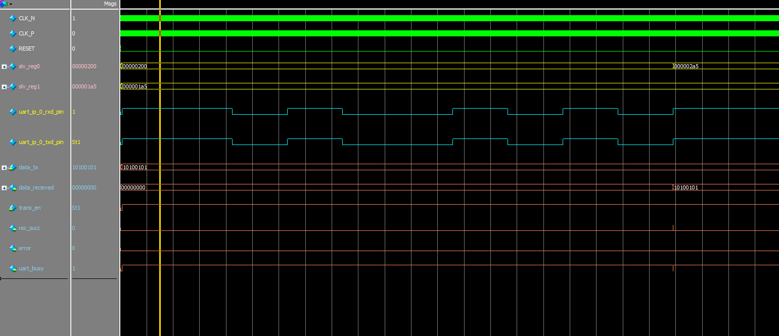
Рис 3.1 Временная диаграмма обмена данными между процессором Microblaze и внешним цифровым устройством с использованием разработанного IP ядра UART
В процессе моделирования был рассмотрен следующий пример: процессор по шине AXI выставляет данные в адресуемый регистр управления slv_reg1(данные для передачи – 8 младших разрядов регистра, сигнал начала передачи – 8-й разряд регистра) для передачи внешнему устройству с помощью IP ядра UART. В файле тестовых воздействий выходной сигнал системы uart_ip_0_txd_pin (выход интерфейса UART) замкнут на входной uart_ip_0_rxd_pin (вход интерфейса UART).
В результате отрабатывается передача данных по линии uart_ip_0_txd_pin и прием по линии uart_ip_0_rxd_pin с задержкой в 1 такт системной частоты. Принятые данные записываются в младшие разряды адресуемого со стороны процессора регистра состояний slv_reg0, что и отображено на временной диаграмме.
4. Исходный код разработанного модуля (описание на языке VerilogHDL)
1) Код верхнего уровня модуля интерфейса UART (файл uart_top.v)
// bit rate: 9600 kbit/sec
// clock: 100 MHz
module uart_top #(parameter FREQ = 100,
parameter RATE = 1,
parameter MAJ_DIV = 128)
(
input clock,
input reset_n,
input data_tx,
output data_recieved,
input trans_en,
output rec_succ,
output error,
output uart_busy,
input rxd,
output txd
);
wire clock;
wire reset_n;
wire [7:0] data_tx;
reg [7:0] data_recieved;
wire trans_en;
reg rec_succ;
reg error;
reg uart_busy;
wire rxd;
wire txd;
// LOCAL PARAMETERS
// FREQ is in MHz
// if FREQ = 100, real frequency is 100 MHz (100 000 000 Hz)
// real rate = 9600*RATE;
// if RATE = 2, real rate is 19200 bod/sec
localparam CNT_PULSES = (FREQ*1000000)/(9600*RATE);
// shift reg for TX
reg [9:0] tx_reg;
reg [13:0] tx_cnt;
reg [1:0] state_tx;
// shift reg for RX
reg [9:0] rx_reg;
reg [13:0] rx_cnt;
reg [1:0] state_rx;
reg [3:0] tx_cnt_bits;
reg [3:0] rx_cnt_bits;
reg rx_maj;
assign txd = tx_reg[0];
majority_scheme #(CNT_PULSES, MAJ_DIV)
majority_scheme_inst(
.clock(clock),
.reset_n(reset_n),
.rx_maj(rx_maj),
.rx_cnt(rx_cnt),
.maj_out_bit(maj_out_bit)
);
always @(posedge clock or negedge reset_n)
if (~reset_n)
begin
tx_reg <= 0;
rx_reg <= 0;
rx_cnt <= 0;
tx_cnt <= 0;
state_tx <= 0;
state_rx <= 0;
uart_busy <= 0;
data_recieved <= 0;
rec_succ <= 0;
rx_maj <= 0;
tx_cnt_bits <= 0;
rx_cnt_bits <= 0;
error <= 0;
end
else
begin
// One pulse
rec_succ <= 0;
// Transmitter
case (state_tx)
// idle
0: begin
if (trans_en)
state_tx <= 1;
end
// register data to transmit
1: begin
uart_busy <= 1;
tx_reg[8:1] <= data_tx;
tx_reg[9] <= 0; // stop bit
tx_reg[0] <= 1; // start bit
state_tx <= 2;
end
// transmit 10 bits
2: begin
if (tx_cnt == 10417)
begin
tx_cnt <= 0;
tx_reg[8:0] <= tx_reg[9:1];
tx_reg[9] <= 0;
tx_cnt_bits <= tx_cnt_bits + 1;
if (tx_cnt_bits == 9)
begin
state_tx <= 0;
uart_busy <= 0;
tx_cnt_bits <= 0;
end
end
else
tx_cnt <= tx_cnt + 1;
end
endcase
// Reciever
case (state_rx)
// idle
0: begin
if (rxd)
state_rx <= 1;
end
// recieve 10 bits
1: begin
rx_maj <= rxd;
if (rx_cnt_bits == 10)
begin
state_rx <= 2;
rx_cnt_bits <= 0;
end
if (rx_cnt == CNT_PULSES)
begin
rx_cnt <= 0;
rx_reg[9] <= maj_out_bit;
rx_reg[8:0] <= rx_reg[9:1];
rx_cnt_bits <= rx_cnt_bits + 1;
end
else
rx_cnt <= rx_cnt + 1;
end
// register recieved data
2: begin
data_recieved <= rx_reg[8:1];
if (~rx_reg[9])
rec_succ <= 1;
else
error <= 1;
state_rx <= 0;
end
endcase
end
endmodule
2) Код мажоритарной схемы приемника модуля UART (файл majority_scheme.v)
module majority_scheme #(parameter CNT_PULSES = 1,
parameter MAJ_DIV = 2)
(
// System
input wire clock,
input wire reset_n,
input wire [13:0] rx_cnt,
input wire rx_maj,
output reg maj_out_bit
);
localparam MIN_CNT_ONES = CNT_PULSES/(64*MAJ_DIV);
reg [2:0] cnt_ones;
always @(posedge clock or negedge reset_n)
if (~reset_n)
begin
maj_out_bit <= 0;
cnt_ones <= 0;
end
else
begin
if (rx_cnt[MAJ_DIV + 5:0] == 7'b0000000)
begin
if (rx_maj)
cnt_ones <= cnt_ones + 1;
else
cnt_ones <= cnt_ones + 0;
end
if (cnt_ones > MIN_CNT_ONES && rx_cnt == CNT_PULSES - 1)
begin
maj_out_bit <= 1;
cnt_ones <= 0;
end
else if (cnt_ones <= MIN_CNT_ONES && rx_cnt == CNT_PULSES - 1)
begin
maj_out_bit <= 0;
cnt_ones <= 0;
end
end
endmodule
3) Код модуля user_logic.v
`uselib lib=unisims_ver
`uselib lib=proc_common_v3_00_a
module user_logic
(
// -- ADD USER PORTS BELOW THIS LINE ---------------
// --USER ports added here
// -- ADD USER PORTS ABOVE THIS LINE ---------------
txd,
rxd,
// -- DO NOT EDIT BELOW THIS LINE ------------------
// -- Bus protocol ports, do not add to or delete
Bus2IP_Clk, // Bus to IP clock
Bus2IP_Resetn, // Bus to IP reset
Bus2IP_Data, // Bus to IP data bus
Bus2IP_BE, // Bus to IP byte enables
Bus2IP_RdCE, // Bus to IP read chip enable
Bus2IP_WrCE, // Bus to IP write chip enable
IP2Bus_Data, // IP to Bus data bus
IP2Bus_RdAck, // IP to Bus read transfer acknowledgement
IP2Bus_WrAck, // IP to Bus write transfer acknowledgement
IP2Bus_Error // IP to Bus error response
// -- DO NOT EDIT ABOVE THIS LINE ------------------
); // user_logic
// -- ADD USER PARAMETERS BELOW THIS LINE ------------
// --USER parameters added here
// -- ADD USER PARAMETERS ABOVE THIS LINE ------------
// -- DO NOT EDIT BELOW THIS LINE --------------------
// -- Bus protocol parameters, do not add to or delete
parameter C_NUM_REG = 2;
parameter C_SLV_DWIDTH = 32;
// -- DO NOT EDIT ABOVE THIS LINE --------------------
// -- ADD USER PORTS BELOW THIS LINE -----------------
// --USER ports added here
// -- ADD USER PORTS ABOVE THIS LINE -----------------
input rxd;
output txd;
// -- DO NOT EDIT BELOW THIS LINE --------------------
// -- Bus protocol ports, do not add to or delete
input Bus2IP_Clk;
input Bus2IP_Resetn;
input [C_SLV_DWIDTH-1: 0] Bus2IP_Data;
input [C_SLV_DWIDTH/8-1: 0] Bus2IP_BE;
input [C_NUM_REG-1: 0] Bus2IP_RdCE;
input [C_NUM_REG-1: 0] Bus2IP_WrCE;
output [C_SLV_DWIDTH-1: 0] IP2Bus_Data;
output IP2Bus_RdAck;
output IP2Bus_WrAck;
output IP2Bus_Error;
// -- DO NOT EDIT ABOVE THIS LINE --------------------
//----------------------------------------------------------------------------
// Implementation
//----------------------------------------------------------------------------
// --USER nets declarations added here, as needed for user logic
// Nets for user logic slave model s/w accessible register example
reg [C_SLV_DWIDTH-1: 0] slv_reg0;
reg [C_SLV_DWIDTH-1: 0] slv_reg1;
wire [1: 0] slv_reg_write_sel;
wire [1: 0] slv_reg_read_sel;
reg [C_SLV_DWIDTH-1: 0] slv_ip2bus_data;
wire slv_read_ack;
wire slv_write_ack;
integer byte_index, bit_index;
// USER logic implementation added here
// user lines
wire [7:0] data_tx;
wire trans_en;
wire [7:0] data_recieved;
wire rec_succ;
wire uart_busy;
wire error;
wire txd;
wire rxd;
assign data_tx = slv_reg1[7:0];
assign trans_en = slv_reg1[8];
uart_top uart_top_inst(
.clock(Bus2IP_Clk),
.reset_n(Bus2IP_Resetn),
.data_tx(data_tx),
.data_recieved(data_recieved),
.trans_en(trans_en),
.rec_succ(rec_succ),
.error(error),
.uart_busy(uart_busy),
.rxd(rxd),
.txd(txd)
);
// ------------------------------------------------------
// Example code to read/write user logic slave model s/w accessible registers
//
// Note:
// The example code presented here is to show you one way of reading/writing
// software accessible registers implemented in the user logic slave model.
// Each bit of the Bus2IP_WrCE/Bus2IP_RdCE signals is configured to correspond
// to one software accessible register by the top level template. For example,
// if you have four 32 bit software accessible registers in the user logic,
// you are basically operating on the following memory mapped registers:
//
// Bus2IP_WrCE/Bus2IP_RdCE Memory Mapped Register
// "1000" C_BASEADDR + 0x0
// "0100" C_BASEADDR + 0x4
// "0010" C_BASEADDR + 0x8
// "0001" C_BASEADDR + 0xC
//
// ------------------------------------------------------
assign
slv_reg_write_sel = Bus2IP_WrCE[1:0],
slv_reg_read_sel = Bus2IP_RdCE[1:0],
slv_write_ack = Bus2IP_WrCE[0] || Bus2IP_WrCE[1],
slv_read_ack = Bus2IP_RdCE[0] || Bus2IP_RdCE[1];
// implement slave model register(s)
always @(posedge Bus2IP_Clk)
begin
if (Bus2IP_Resetn == 1'b0)
begin
slv_reg0 <= 0;
slv_reg1 <= 0;
end
else
begin
slv_reg0[7:0] <= data_recieved;
slv_reg0[8] <= rec_succ;
slv_reg0[9] <= uart_busy;
slv_reg[10] <= error;
case (slv_reg_write_sel)
2'b10:
for (byte_index = 0; byte_index <= (C_SLV_DWIDTH/8)-1; byte_index = byte_index+1)
if (Bus2IP_BE[byte_index] == 1)
slv_reg0[(byte_index*8) +: 8] <= Bus2IP_Data[(byte_index*8) +: 8];
2'b01:
for (byte_index = 0; byte_index <= (C_SLV_DWIDTH/8)-1; byte_index = byte_index+1)
if (Bus2IP_BE[byte_index] == 1)
slv_reg1[(byte_index*8) +: 8] <= Bus2IP_Data[(byte_index*8) +: 8];
default: begin
slv_reg0 <= slv_reg0;
slv_reg1 <= slv_reg1;
end
endcase
end
end // SLAVE_REG_WRITE_PROC
// implement slave model register read mux
always @(slv_reg_read_sel or slv_reg0 or slv_reg1)
begin
case (slv_reg_read_sel)
2'b10: slv_ip2bus_data <= slv_reg0;
2'b01: slv_ip2bus_data <= slv_reg1;
default: slv_ip2bus_data <= 0;
endcase
end // SLAVE_REG_READ_PROC
// ------------------------------------------------------------
// Example code to drive IP to Bus signals
// ------------------------------------------------------------
assign IP2Bus_Data = (slv_read_ack == 1'b1)? slv_ip2bus_data: 0;
assign IP2Bus_WrAck = slv_write_ack;
assign IP2Bus_RdAck = slv_read_ack;
assign IP2Bus_Error = 0;
endmodule
Приложение 1. Создание проекта в Xilinx Platform Studio

