


ѕри виконанн≥ даноњ частини ƒ –, €ка передбачаЇ анал≥з файл≥в з дов≥дниковими даними на нап≥впров≥дниковий елемент, до виконаного завданн€ додаЇтьс€ роздрук≥вка початкового файлу (Data Sheet).
3.3.1.ќгл€д файл≥в з дов≥дниковими даними. ƒов≥дников≥ дан≥ на нап≥впров≥дников≥ прилади залежно в≥д виробника можуть дещо в≥др≥зн€тис€ за вигл€дом та стилем њх представленн€, але загальна структура збер≥гаЇтьс€. «овн≥шн≥й вигл€д стор≥нки з Data Sheet нап≥впров≥дникових елемент≥в р≥зних ф≥рм виробник≥в з по€сненн€м основних структурних частин наведен≥ в ƒодатку 4.
”крањномовний переклад електричних параметр≥в прилад≥в доц≥льно представл€ти у форм≥ таблиць, аналог≥чних наведеним в дов≥дникових даних.
јнал≥з виконуЇтьс€ дл€ тих характеристик ≥ залежностей, €к≥ вказан≥ в завданн≥ до ƒ – (по кожному приладу викладачем зд≥йснюЇтьс€ адаптац≥€ та детал≥зац≥€ завданн€).
јнал≥з особливостей побудови, функц≥онуванн€ приладу, сфер його застосуванн€ охоплюЇ практично вс≥ дан≥, наведен≥ у файлах Data Sheet дл€ приладу.
¬ ход≥ виконанн€ завдань з ƒ – за наведеними характеристиками необх≥дно обрахувати т≥ чи ≥нш≥ параметри.
ƒал≥ розгл€даЇтьс€ принцип розрахунку цих параметр≥в.
3.1.2. –озрахунок параметр≥в елемент≥в за вольт-амперними характеристиками.
ѕри розгл€д≥ та анал≥з≥ параметр≥в та характеристик приладу викладачем може бути поставлена задача розрахунку певних параметр≥в за наведеними вольт-амперними та ≥ншими характеристиками. ƒал≥ навод€тьс€ основн≥ формули, що використовуютьс€ при цьому.
—татичний оп≥р приладу у в≥дкритому або закритому стан≥ визначаЇтьс€ €к в≥дношенн€ напруги до струму в ф≥ксован≥й точц≥ на вольт-амперн≥й характеристиц≥:  .
.
–озрахунок динам≥чного опору приладу починаЇтьс€ з визначенн€ за його ¬ј’ прирост≥в напруги та в≥дпов≥дних прирост≥в струму в околиц≥ заданоњ точки (точка ј на рис. 1 може бути задана шл€хом вказуванн€ струму чи напруги в н≥й). ѕ≥сл€ цього знаходитьс€ в≥дношенн€ даних прирост≥в за формулою:  .
.

–ис. 1. ƒо визначенн€ динам≥чного опору елементу
¬ольт-амперн≥ характеристики зазвичай навод€тьс€ у вигл€д≥ двох с≥мейств характеристик Ц окремо дл€ пр€моњ напруги та струму та окремо дл€ зворотноњ (рис. 2 а) та б) в≥дпов≥дно).
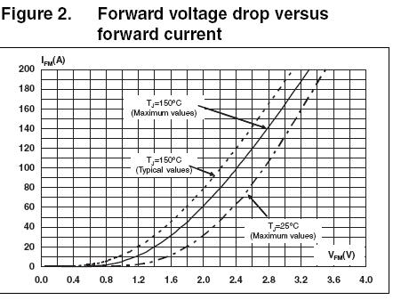
–ис. 2.а) «алежн≥сть пад≥нн€ пр€моњ напруги в≥д пр€мого струму

–ис. 2.б) “ипова залежн≥сть зворотного струму в≥д зворотноњ напруги
як видно з рис. 2 форми представленн€ характеристик у р≥зник виробник≥в Ї дещо р≥зними, тому рекомендовано ор≥Їнтуватис€ на символьн≥ позначенн€ параметр≥в по ос€х та њх по€сненн€.
“емператури pn-переходу, дл€ €ких зн€т≥ дан≥ характеристики, вказуютьс€ або безпосередньо на характеристиках, або у форм≥ зносок пор€д з ними.
ќдиниц≥ вим≥рюванн€ параметр≥в вказуютьс€ в дужках по ос€х безпосередньо б≥л€ параметр≥в.
≤ншою характеристикою д≥од≥в Ї вольт-фарадна характеристика Ц залежн≥сть Їмност≥ pn-переходу в≥д прикладеноњ до д≥ода зворотноњ напруги.
«а нею можна визначити на ск≥льки зм≥нитьс€, наприклад, Їмн≥сть при зм≥н≥ напруги на вказане значенн€. Ќа рис. 3 наведено фрагмент Data Sheet д≥ода з вольт-фарадною характеристикою. Ќа граф≥ку вказана температура переходу, дл€ €коњ зн€та в≥дпов≥дна залежн≥сть -  .
.
|
|
|

–ис. 3. “ипова залежн≥сть Їмност≥ pn -переходу в≥д зворотноњ напруги
ƒл€ б≥пол€рних транзистор≥в одн≥Їю з основних характеристик Ї залежн≥сть струму колектора в≥д напруги база-ем≥тер (рис. 4) Ц прох≥дна характеристика або передавальна характеристика.

–ис. 4.а) Ќапруга база-ем≥тер €к функц≥€ в≥д колекторного струму; типов≥ значенн€
Ќа граф≥ках рис. 4 вказано умови вим≥рювань: три температури навколишнього середовища  Ц
Ц  та напруга колектор-ем≥тер
  .
.
р≥м того, дл€ б≥пол€рного транзистора можна побудувати прох≥дну (передавальну характеристику) так, €к це показано на рис. 4.б.

–ис. 4. б) ѕринцип побудови прох≥дноњ характеристики транзистора
ƒл€ б≥пол€рних транзистор≥в важливим параметром Ї коеф≥ц≥Їнт передач≥ струму  . ƒл€ нього значенн€ вказуютьс€ або в таблиц€х, або у вигл€д≥ граф≥к≥в типу рис. 5. Ќа рис. 5 вказано тривал≥сть в≥дкритого стану транзистора
  в мкс, коеф≥ц≥Їнт заповненн€ ≥мпульс≥в
  , де “ Ц пер≥од сл≥дуванн€ ≥мпульс≥в, температуру pn -переходу та напругу колектор-ем≥тер.

–ис. 5. оеф≥ц≥Їнт передач≥ пост≥йного струму €к функц≥€ в≥д струму колектора; типов≥ значенн€
ƒл€ б≥пол€рних транзистор≥в, так само €к ≥ дл€ д≥од≥в, також можуть наводитись залежност≥ Їмностей переход≥в в≥д напруги ≥ принцип роботи з цими залежност€ми такий же.
якщо дл€ б≥пол€рного транзистора наведен≥ граф≥ки залежностей струму колектора в≥д напруги колектор-ем≥тер, то за ними можна визначити положенн€ робочоњ точки дл€ заданих значень напруги та струму (див. рис. 6).

а) б)
–ис. 6. ƒо побудови навантажувальноњ характеристик, динам≥чноњ характеристики та визначенн€ положенн€ робочоњ точки транзистора
Ќа рис. 6 показано принцип побудови навантажувальноњ характеристики з використанн€м наступного р≥вн€нн€:
 . (1)
. (1)
—п≥вв≥дношенн€ (1) Ї р≥вн€нн€м навантажувальноњ характеристики - пр€моњ, €ка будуЇтьс€ на вих≥дних характеристиках схеми ≥ проходить через дв≥ точки з наступними координатами (рис. 8):
1) точка на ос≥ струм≥в з  ;
;
2) точка на ос≥ напруг з  .
.
—укупн≥сть точок перетину статичних характеристик транзистора ≥з навантажувальною пр€мою (д≥л€нка ј¬ рис. 6) називаЇтьс€ динам≥чною характеристикою транзистора.
ƒл€ визначенн€ положенн€ робочоњ точки на вх≥дних характеристиках (рис.6,а) враховуЇтьс€ початкове значенн€ напруги м≥ж базою та ем≥тером транзистора  , €ке задаЇтьс€ джерелом живленн€ та вх≥дним резистивним д≥льником. √рафоанал≥тичним методом, шл€хом проекц≥њ точки на характеристику знаходитьс€ в≥дпов≥дний струм бази
  (рис. 6,а). ÷ей струм, в свою чергу, буде визначати положенн€ робочоњ точки на вих≥дних характеристиках, €ке визначаЇтьс€ €к точка – перетину навантажувальноњ пр€моњ з характеристикою, що в≥дпов≥даЇ струму (рис. 6,б). ѕроекц≥Їю даноњ точки на в≥сь напруг та струм≥в визначаютьс€ њњ параметри за вих≥дними характеристиками транзистора: напруга м≥ж колектором та ем≥тером
  ≥ струм колектора
  (див. рис. 6,б). «найдене положенн€ робочоњ точки – транзистора характеризуЇ його робочий режим по пост≥йному струму.
якщо в завданн≥ задано значенн€ напруги колектор-ем≥тер та значенн€ струму, то за ними будуЇтьс€ навантажувальна пр€ма ≥ дал≥ знаходитьс€ робоча точка.
|
|
|
¬ польових транзисторах важливими характеристиками Ї стоков≥ (залежн≥сть струму стоку в≥д напруги ст≥к-вит≥к) та стоково-затворн≥ (залежн≥сть струму стоку в≥д напруги затвор-вит≥к) характеристики, причому останн≥ можуть бути побудованими за стоковими так, €к це показано на рис. 7.

а) б)
–ис. 7. —токов≥ (а) та стоково-затворна (б) характеристики польового транзистора ѕ601(ј,Ѕ)
«алежн≥сть струму стоку в≥д зворотноњ напруги м≥ж затвором та витоком  (рис. 7,б) будуютьс€ наступним чином. ƒл€ ф≥ксованого значенн€ напруги м≥ж стоком та витоком
  (на рис. 7,а обрано напругу 10¬) граф≥чним способом визначаютьс€ значенн€ струму стоку при р≥зних значенн€х напруги
  . ќтриман≥ значенн€ струму перенос€тьс€ на в≥сь струму стоково-затворноњ характеристики (на рис. 7 перенесенн€ точок показано пунктиром). ƒал≥, визначаютьс€ положенн€ точок характеристики залежно в≥д значень напруги затвор-вит≥к, що вказан≥ над стоковими характеристиками ≥ в≥дкладаютьс€ на ос≥ напруг стоково-затворноњ характеристики. «а отриманою множиною точок будуЇтьс€ залежн≥сть.
ƒл€ б≥пол€рних транзистор≥в з ≥зольованим затвором (IGBT) одн≥Їю з характеристик Ї перех≥дна (передавальна) Ц залежн≥сть струму колектора в≥д напруги затвор-ем≥тер (рис. 11). ¬она може бути побудована за вих≥дними характеристиками IGBT аналог≥чно до побудови стоково-затворних характеристик.

–ис.7. ѕерех≥дна (передавальна) характеристика IGBT
ѕерех≥дна характеристика IGBT будуЇтьс€ аналог≥чно перех≥дн≥й характеристиц≥ б≥пол€рного транзистора (див. рис. 4.б).
ќдн≥Їю з важливих характеристик нап≥впров≥дникових прилад≥в Ї область безпечноњ роботи приладу (Safe Operating Area - SOA) Ц область значень струму та напруги, при комб≥нац≥њ €ких прилад здатен тривало функц≥онувати без пошкодженн€ ≥ виходу з ладу (приклад дл€ IGBT наведено на рис. 8). ‘орма даноњ област≥ суттЇво залежить в≥д умов роботи приладу, зокрема в≥д тривалост≥ в≥дкритого стану транзистора, €к у наведеному на рис. 8 приклад≥.
“ривал≥сть в≥дкритого стану приладу вказуЇтьс€ на граф≥ках або в одиниц€х вим≥рюванн€ часу Ц м≥кросекунди, м≥л≥секунди, або у в≥дносних одиниц€х , де  - коеф≥ц≥Їнт заповненн€ ≥мпульс≥в, - тривал≥сть ≥мпульсу, тобто тривал≥сть в≥дкритого стану приладу, “ Ц пер≥од сл≥дуванн€ ≥мпульс≥в.
’арактеристика на рис.5 побудована дл€ температури корпусу (temperature of case) “— =250—, температури pn -переход≥в транзистора Tj =1500— та одиничного ≥мпульсу (single pulse) керуванн€, що подаЇтьс€ на транзистор ≥ визначаЇ його в≥дкритий стан. ‘орма залежност≥ визначаЇтьс€ тривал≥стю ≥мпульсу.
„им довше транзистор або д≥од знаходитьс€ у в≥дкритому стан≥, тим менш≥ струми в≥н здатен пропускати при тих же значенн€х напруги. ÷е обумовлено його можлив≥стю розс≥ювати обмежену енерг≥ю, що вид≥л€Їтьс€ у вигл€д≥ тепла. ќск≥льки миттЇва потужн≥сть визначаЇтьс€ €к добуток миттЇвого струму на миттЇву напругу, то при зростанн≥ тривалост≥ в≥дкритого стану сумарна енерг≥€ при одних ≥ тих же значенн€х струму та напруги р≥зко зростаЇ ≥ може перевищити допустиму. “ому струми ≥ напруги обмежуютьс€, що в≥дображаЇтьс€ пунктирною л≥н≥Їю.
р≥м того, в де€ких д≥апазонах напруг та струм≥в необх≥дно враховувати вплив опору елементу у в≥дкритому стан≥, про що зазвичай пишуть на граф≥ках.
¬ процес≥ анал≥зу област≥ безпечноњ роботи необх≥дно вказати в≥д €ких параметр≥в залежить њњ форма ≥ €к саме.

| –ис. 8. ќбласть безпечноњ роботи транзистора в координатах залежност≥ струму колектора ≤— в≥д напруги колектор-ем≥тер VCE |
¬ ≥деальному випадку область безпечноњ роботи повинна бути пр€мокутною, до чого власне ≥ прагнуть виробники нап≥впров≥дникових прилад≥в, розробл€ючи нов≥ структури та застосовуючи р≥зноман≥тн≥ технолог≥чн≥ п≥дходи.
ƒал≥ наведено множину типових параметр≥в нап≥впров≥дникових прилад≥в. «важте, що виробники активно використовують додатков≥ параметри, €к≥ б≥льш детально розкривають можливост≥ прилад≥в, зокрема њх динам≥чн≥ характеристики.
|
|
|
ƒо динам≥чних характеристик належать тривалост≥ вмиканн€ та вимиканн€, часов≥ затримки, енерг≥њ, що розс≥юютьс€ в прилад≥ при вмиканн≥, вимиканн≥, тривалому перебуванню у в≥дкритому стан≥, Їмност≥ переход≥в, величини накопичених на переходах зар€д≥в ≥ т.≥н. ¬с≥ ц≥ параметри детально в≥дображен≥ в √ќ—“-ах на нап≥впров≥дников≥ прилади, що додаютьс€.
“ипов≥ параметри ƒ≤ќƒ≤¬ ( √ќ—“ 25529-82 )
“аблиц€ 1.1. ќсновн≥ параметри д≥од≥в та њх позначенн€
| ѕараметр | —имвольне позначенн€ | ¬изначенн€ |
| ѕост≥йна пр€ма напруга (Forward continuous voltage) | 
| ѕост≥йна напруга на д≥од≥ при заданому пр€мому струм≥ нап≥впров≥дникового д≥ода. |
| ѕост≥йна зворотна напруга(Reverse continuous voltage) | 
| ѕост≥йна напруга, прикладена до д≥ода у зворотному напр€мку. |
| ѕост≥йний пр€мий струм (Forward continuous current) | 
| ѕост≥йний струм, що прот≥каЇ через д≥од у пр€мому напр€мку. |
| ѕост≥йний зворотний струм(Reverse continuous current) | 
| ѕост≥йний струм, що прот≥каЇ через д≥од у зворотному напр€мку при задан≥й зворотн≥й напруз≥. |
| —ередн≥й пр€мий струм (Average forward current) | 
| «наченн€ пр€мого струму, усереднене за пер≥од. |
| ƒиференц≥альний оп≥р д≥од (Differential resistance) | 
| ¬≥дношенн€ малого приросту напруги на д≥од≥ до малого приросту його струму при заданому режим≥. ћоже визначатис€, €к на пр€м≥й д≥л€нц≥ ¬ј’ д≥ода  , так ≥ на зворотн≥й , так ≥ на зворотн≥й  . .
|
| ЅарТЇрна Їмн≥сть (Їмн≥сть p-n переходу) (Junction capacitance) | 
| значенн€ Їмност≥ м≥ж виводами д≥ода в заданому режим≥ без врахуванн€ Їмност≥ корпусу. |
“аблиц€ 1.2. ѕараметри випр€мних д≥од≥в та њх позначенн€*
| ѕараметр | —имвольне позначенн€ | ¬изначенн€ |
| –обоча ≥мпульсна зворотна напруга випр€много д≥ода (Working peak reverse voltage) | 
| Ќайб≥льше миттЇве значенн€ зворотноњ напруги випр€много д≥ода без врахуванн€ перех≥дних напруг (€к пер≥одичних, так ≥ непер≥одичних). |
| ѕер≥одична ≥мпульсна зворотна напруга(Repetitive peak reverse voltage) | 
| Ќайб≥льше миттЇве значенн€ зворотноњ напруги випр€много д≥ода з урахуванн€м перех≥дних напруг, що повторюютьс€. |
| Ќепер≥одична ≥мпульсна зворотна напруга(Non-repetitive (surge) reverse voltage) | 
| Ќайб≥льше миттЇве значенн€ зворотноњ напруги випр€много д≥ода з урахуванн€м непер≥одичних перех≥дних напруг. |
| √ранична (порогова) напруга випр€много д≥ода (Threshold voltage) | 
| «наченн€ пост≥йноњ пр€моњ напруги випр€много д≥ода в точц≥ перетину з в≥ссю напруг пр€моњ л≥н≥њ, що апроксимуЇ вольт-амперну характеристику в област≥ великих струм≥в. |
| ƒ≥юча зворотна напруга (RMS voltage) | 
| ƒ≥юче значенн€ зворотноњ напруги д≥ода за пер≥од. |
| ѕер≥одичний ≥мпульсний пр€мий струм (Repetitive peak forward current) | 
| Ќайб≥льше миттЇве значенн€ пр€мого струму д≥ода, включаючи пер≥одичн≥ перех≥дн≥ струми. |
| ”дарний пр€мий струм випр€много д≥ода | 
| —трум, при прот≥канн≥ €кого перевищуЇтьс€ максимально допустима температура переходу, але €кий за час терм≥ну служби д≥ода зТ€вл€Їтьс€ р≥дко з обмеженою к≥льк≥стю повтор≥в ≥ обумовлений незвичними режимами роботи схеми. |
| ƒ≥ючий пр€мий струм д≥ода(RMS forward current) | 
| ƒ≥юче значенн€ пр€мого струму д≥ода за пер≥од. |
| ѕер≥одичний ≥мпульсний зворотний струм (Repetitive peak reverse current) | 
| «наченн€ зворотного струму д≥ода, обумовлене ≥мпульсною зворотною напругою, що повторюЇтьс€. |
| —ередн≥й зворотний струм(Average reverse current) | 
| —ереднЇ за пер≥од значенн€ зворотного струму д≥ода. |
| —ередн≥й випр€млений струм д≥ода(Average output rectified current) | 
| —ереднЇ за пер≥од значенн€ пр€мого та зворотного струм≥в д≥ода. |
| ƒинам≥чний оп≥р випр€много д≥ода (Slope resistance) | 
| ќп≥р, що визначаЇтьс€ нахилом пр€моњ, €ка апроксимуЇ пр€му г≥лку вольт-амперноњ характеристики д≥ода. |
ѕерех≥дн≥ пер≥одичн≥ напруги зазвичай визначаютьс€ схемою та параметрами д≥ода.
|
|
|
ѕерех≥дн≥ непер≥одичн≥ напруги обумовлен≥ зазвичай зовн≥шньою причиною ≥ передбачаЇтьс€, що њх д≥€ зникаЇ повн≥стю до по€ви наступноњ перех≥дноњ напруги.
“аблиц€ 1.4. ѕараметри ≥мпульсних д≥од≥в та њх позначенн€
| “ерм≥н | —имвольне позначенн€ | ¬изначенн€ |
| ≤мпульсна пр€ма напруга (Peak forward voltage) | 
| Ќайб≥льше миттЇве значенн€ пр€моњ напруги, обумовлене пр€мим ≥мпульсним струмом д≥ода заданого значенн€. |
| ≤мпульсна зворотна напруга (Peak reverse voltage) | 
| Ќайб≥льше миттЇве значенн€ зворотноњ напруги. |
| «агальна Їмн≥сть (Terminal capacitance) | 
| ™мн≥сть, €ка вим≥рюЇтьс€ м≥ж виводами д≥ода при задан≥й напруз≥ й частот≥. |
| „ас пр€мого в≥дновленн€ (час встановленн€ пр€моњ напруги або час в≥дновленн€ пр€мого опору) (Forward recovery time) | 
| ≤нтервал часу, прот€гом €кого в≥дбуваЇтьс€ вмиканн€ д≥ода ≥ пр€ма напруга на ньому встановлюЇтьс€ в≥д значенн€, р≥вного нулю, до заданого усталеного значенн€. |
| „ас зворотного в≥дновленн€ (Reverse recovery time) | 
| ≤нтервал часу з моменту зм≥ни струмом д≥оду свого напр€мку з пр€мого на зворотн≥й до моменту дос€гненн€ зворотн≥м струмом заданого значенн€. |
| «ар€д в≥дновленн€ д≥ода (зар€д перемиканн€) (Recovered charge) | 
| ѕовний зар€д д≥ода, що перехо≠дить до зовн≥шнього кола при перемиканн≥ д≥ода з заданого значенн€ пр€мого струму на задане значенн€ зворотноњ напруги. |
“аблиц€ 1.7. ѕараметри стаб≥л≥трон≥в та њх позначенн€
| “ерм≥н | —имвольне позначенн€ | ¬изначенн€ |
| Ќапруга стаб≥л≥зац≥њ (Working voltage (of voltage regulator diode)) | 
| Ќапруга на стаб≥л≥трон≥ при заданому струм≥ стаб≥л≥зац≥њ. |
| ƒопустиме в≥дхиленн€ напруги стаб≥л≥зац≥њ в≥д ном≥нальноњ | - | ћаксимально допустиме в≥дхиленн€ напруги стаб≥л≥зац≥њ в≥д ном≥нальноњ дл€ стаб≥л≥трон≥в даного типу. |
| —трум стаб≥л≥зац≥њ (Continuous current within the working voltage range) | 
| «наченн€ пост≥йного струму, що прот≥каЇ через стаб≥л≥трон в режим≥ стаб≥л≥зац≥њ. |
| ћаксимальний струм стаб≥л≥зац≥њ | - | ћаксимально допустимий р≥вень струму через стаб≥л≥трон, перевищенн€ €кого призводить до виходу його з ладу. |
| ћ≥н≥мальний струм стаб≥л≥зац≥њ | - | ћ≥н≥мальний р≥вень струму через стаб≥л≥трон, що визначаЇ нижню границю його робочого д≥апазону, тобто зниженн€ струму нижче цього р≥вн€ призводить до виходу стаб≥л≥трону з режиму стаб≥л≥зац≥њ. |
| ≤мпульсний струм стаб≥л≥зац≥њ | 
| Ќайб≥льше миттЇве значенн€ струму стаб≥л≥зац≥њ стаб≥л≥зац≥њ. |
| ƒиференц≥альний оп≥р (Differential resistance within the working voltage range) | 
| ƒиференц≥альний оп≥р при заданому струм≥ стаб≥л≥зац≥њ стаб≥л≥трона. |
| “емпературний коеф≥ц≥Їнт напруги стаб≥л≥зац≥њ (Temperature coefficient of working voltage) | 
| ¬≥дношенн€ в≥дносноњ зм≥ни напруги стаб≥л≥зац≥њ до абсолютноњ зм≥ни температури навколишнього середовища при пост≥йному струм≥ стаб≥л≥зац≥њ. |
| „ас вмиканн€ (Turn-on time) | 
| ≤нтервал часу, що в≥драховуЇтьс€ в≥д моменту перемиканн€ стаб≥л≥трона в≥д значенн€ заданоњ напруги до моменту дос€гненн€ усталеноњ напруги стаб≥л≥зац≥њ. |
“ипов≥ параметри Ѕ≤ѕќЋя–Ќ»’ “–јЌ«»—“ќ–≤¬ ( √ќ—“ 20003-74 )
“аблиц€ 3.1. ќсновн≥ параметри ¬ј’ б≥пол€рного транзистора
| “ерм≥н | —имвольне позначенн€ | ¬изначенн€ | |
| ”кр. | јнгл. | ||
| Ќапруга колектор-ем≥тер насиченн€(Saturation collector-emitter voltage) | 
| 
| Ќапруга м≥ж виводам колектор та ем≥тер транзистора в режим≥ насиченн€ при заданих струмах бази та колектора |
| Ќапруга база-ем≥тер насиченн€(Saturation base-emitter voltage) | 
| 
| Ќапруга м≥ж виводам база та ем≥тер транзистора в режим≥ насиченн€ при заданих струмах бази та колектора |
| ѕост≥йна напруга колектор-база(Collector-base (d.c.) voltage) | 
| 
| ѕост≥йна напруга м≥ж виводами колектор та база. якщо напруга задаЇтьс€ при певному струм≥ колектора ≥ нульовому струм≥ ем≥тера, використовуЇтьс€ позначенн€ 
|
| ѕост≥йна напруга колектор-ем≥тер(Collector-emitter (d.c.) voltage) | 
| 
| ѕост≥йна напруга м≥ж виводами колектор та ем≥тер. якщо напруга задаЇтьс€ при певному струм≥ колектора ≥ нульовому струм≥ бази, використовуЇтьс€ позначенн€ 
|
| ѕост≥йна напруга ем≥тер-база(Emitter-base (d.c.) voltage) | 
| 
| ѕост≥йна напруга м≥ж виводами ем≥тер та база. якщо напруга задаЇтьс€ при певному струм≥ ем≥тера ≥ нульовому струм≥ колектора, використовуЇтьс€ позначенн€ 
|
| «воротний струм колектора(Collector cut-off current) | 
| 
| —трум через колекторний перех≥д при задан≥й зворотн≥й напруз≥ колектор-база та роз≥мкнутому ем≥терному вивод≥ |
| «воротний струм бази(Emitter cut-off current) | 
| 
| —трум через ем≥терний перех≥д при задан≥й зворотн≥й напруз≥ ем≥тер-база та роз≥мкнутому колекторному вивод≥ |
| ѕост≥йний струм колектора(Collector (d.с.) current) | 
| 
| ѕост≥йний струм, що прот≥каЇ через колекторний перех≥д |
| ѕост≥йний струм бази(Base (d.с.) current) | 
| 
| ѕост≥йний струм, що прот≥каЇ через базовий вив≥д |
*
|
|
|
“аблиц€ 3.2. ќсновн≥ динам≥чн≥ параметри Ѕ“
| “ерм≥н | —имвольне позначенн€ | ¬изначенн€ | |
| ”кр. | јнгл. | ||
| „ас вмиканн€ (Turn-on time) | 
| 
| ≤нтервал часу, що визначаЇтьс€ сумою часу затримки та часу наростанн€ |
| „ас наростанн€(Rise time) | Ц | 
| ≤нтервал часу м≥ж моментами наростанн€ фронту вих≥дного ≥мпульсу в≥д значенн€, що в≥дпов≥даЇ 10 % його ампл≥туди, до значенн€ в 90 % його ампл≥туди |
| „ас вимиканн€ (Turn-off time) | 
| 
| ≤нтервал часу м≥ж моментом подач≥ на базу ≥мпульсу запиранн€ та моментом, коли напруга на колектор≥ транзистора дос€гне значенн€, що в≥дпов≥даЇ 10 % в≥д њњ ампл≥тудного значенн€ |
| √ранична частота коеф≥ц≥Їнта передач≥ за струмом (Transition frequency) | 
| 
| „астота, при €к≥й модуль коеф≥ц≥Їнта передач≥ струму в схем≥ з≥ сп≥льним ем≥тером наближаЇтьс€ до 1, тобто 
|
| „ас розсмоктуванн€(Carrier storage time) | 
| 
| ≤нтервал часу в≥д моменту подач≥ на транзистор замираючого ≥мпульсу до моменту, коли напруга на колектор≥ дос€гне заданого значенн€ |
| „ас спаданн€(Fall time) | 
| 
| ≤нтервал часу м≥ж моментами спаданн€ зр≥зу вих≥дного ≥мпульсу в≥д значенн€, р≥вного 90 % в≥д його ампл≥туди, до значенн€ в 10 % його ампл≥туди |
| ™мн≥сть ем≥терного переходу(Emitter capacitance) | 
| 
| ™мн≥сть м≥ж виводами ем≥тер та база транзистора при заданих зворотн≥й напруз≥ ем≥тер-база та роз≥мкнутому колекторному кол≥ |
| ™мн≥сть колекторного переходу(Collector capacitance) | 
| 
| ™мн≥сть м≥ж виводами колектор та база транзистора при заданих зворотн≥й напруз≥ колектор-база та роз≥мкнутому ем≥терному кол≥ |
| ѕост≥йна потужн≥сть енерг≥њ, що розс≥юЇтьс€ в транзистор≥(Total input power (d.c.) to all electrodes або Total power dissipation) | 
| 
| —умарне значенн€ потужност≥ пост≥йноњ енерг≥њ, що розс≥юЇтьс€ в транзистор≥ |
| —ередн€ потужн≥сть енерг≥њ, що розс≥юЇтьс€ в транзистор≥(Total input power (average) to all electrodes) | 
| 
| ”середнене за пер≥од значенн€ потужност≥ енерг≥њ, що розс≥юЇтьс€ в транзистор≥ |
| ѕотужн≥сть ≥мпульсноњ енерг≥њ, що розс≥юЇтьс€ в транзистор≥(Peak power dissipation) | 
| 
| Ц |
“аблиц€ 3.3. —истема h-параметр≥в б≥пол€рного транзистора
| “ерм≥н | —имвольне позначенн€ | ¬изначенн€ | |
| ”кр. | јнгл. | ||
| ¬х≥дний оп≥р транзистора в режим≥ малого сигналу(Small-signal value of the short-circuit input impedance) | 
|
| в≥дношенн€ зм≥ни напруги на вход≥ до зм≥ни вх≥дного струму, €ка њњ викликала, в режим≥ короткого замиканн€ за зм≥нним струмом на виход≥ транзистора:  при при  за зм≥нним струмом за зм≥нним струмом
|
| ¬их≥дна повна пров≥дн≥сть транзистора в режим≥ малого сигналу(Small-signal value of the open-circuit output admittance) | 
|
| ¬≥дношенн€ зм≥ни вих≥дного струму до зм≥ни вих≥дноњ напруги, що њњ викликала, в режим≥ холостого ходу вх≥дного кола за зм≥нним струмом:  при при  за зм≥нним струмом за зм≥нним струмом
|
| оеф≥ц≥Їнт зворотного звТ€зку за напругою в режим≥ малого сигналу(Small-signal value of the open-circuit reverse voltage transfer ratio) | 
|
| ¬≥дношенн€ зм≥ни напруги на вход≥ до зм≥ни напруги на виход≥, €ка њњ викликала, в режим≥ холостого ходу вх≥дного кола за зм≥нним струмом:  при за зм≥нним струмом при за зм≥нним струмом
|
| оеф≥ц≥Їнт передач≥ струму в режим≥ малого сигналу(Small-signal value of the short-circuit forward current transfer ratio) | 
|
| ¬≥дношенн€ зм≥ни вих≥дного струму транзистора до зм≥ни вх≥дного струму, €ка њњ викликала, в режим≥ короткого замиканн€ вих≥дного кола по зм≥нному струму:  при за зм≥нним струмом при за зм≥нним струмом
|
“ипов≥ параметри ѕќЋ№ќ¬»’ “–јЌ«»—“ќ–≤¬ ( √ќ—“ 19095-73 )
“аблиц€ 3.6. ќсновн≥ параметри польових транзистор≥в
| “ерм≥н | —имвольне позначенн€ | ¬изначенн€ | |
| ”кр. | јнгл. | ||
ѕочатковий струм стоку
(Drain current for  ) )
| 
| 
| —трум стоку при затвором та витоком р≥вн≥й нулю ≥ при напруз≥ на стоц≥, р≥вн≥й чи б≥льш≥й за напругу насиченн€ |
| —трум стоку (Drain current) | 
| 
| —трум, що прот≥каЇ в кол≥ ст≥к-вит≥к при напруз≥ ст≥к-вит≥к б≥льш≥й чи р≥вн≥й напруз≥ насиченн€ та при задан≥й напруг≥ затвор-вит≥к |
| —трум затвора (Gate current) | 
| 
| Ц |
| —трум вит≥канн€ затвора (Gate leakage current) | 
| 
| —трум затвора при задан≥й напруз≥ м≥ж затвором та вс≥ма ≥ншими виводами транзистора, замкнутими м≥ж собою |
| Ќапруга в≥дс≥чки (Gate-source cut-off voltage) | 
| 
| Ќапруга м≥ж затвором ≥ витоком польового транзистора з керуючим p-n-переходом або з ≥зольованим затвором, що працюЇ в режим≥ зб≥дненн€, при €кому струм стоку дос€гаЇ встановленого м≥н≥мального значенн€ |
| Ќапруга ст≥к-вит≥к (Drain-source (d.c.) voltage) | 
| 
| Ц |
| Ќапруга затвор-вит≥к (Gate-source (d.c.) voltage) | 
| 
| Ц |
| Ќапруга затвор-ст≥к (Gate-drain (d.c.) voltage) | 
| 
| Ц |
| Ќапруга пробою затвора (Gate-source breakdown voltage) | 
| 
| Ќапруга пробою затвор-вит≥к при замкнених виводах стоку та витоку |
| Ќапруга пробою затвор-ст≥к (Gate-drain breakdown voltage) | 
| 
| Ц |
| ћодуль повноњ пров≥дност≥ пр€моњ передач≥ (Modulus of the short-circuit forward transfer admittance) | 
| 
| Ц |
“аблиц€ 3.7. ќсновн≥ динам≥чн≥ параметри польових транзистор≥в
| “ерм≥н | —имвольне позначенн€ | ¬изначенн€ | |
| ”кр. | јнгл. | ||
| ¬х≥дна Їмн≥сть (Input capacitance) | 
| 
| ™мн≥сть м≥ж затвором та витоком при короткому замиканн≥ за зм≥нним струмом на виход≥ в схем≥ з≥ сп≥льним витоком |
| ѕрох≥дна Їмн≥сть (Reverce transfer capacitance) | 
| 
| ™мн≥сть м≥ж затвором та стоком при короткому замиканн≥ за зм≥нним струмом на вход≥ в схем≥ з≥ сп≥льним витоком |
| ¬их≥дна Їмн≥сть (Output capacitance) | 
| 
| ™мн≥сть м≥ж стоком ≥ витоком при короткому замиканн≥ за зм≥нним струмом на вход≥ в схем≥ з≥ сп≥льним витоком |
| оеф≥ц≥Їнт шуму (Noise figure) | 
| 
| ¬≥дношенн€ повноњ потужност≥ шум≥в на виход≥ польового транзистора до т≥Їњ њњ частини, €ка викликана тепловими шумами опору джерела сигналу |
| ƒопустима потужн≥сть розс≥юваноњ енерг≥њ (Allowable power dissipation) | 
| 
| Ц |
| “емпература переходу (Junction temperature) | Ц | 
| Ц |
| “емпература збер≥ганн€ (Storage temperature) | Ц | 
| Ц |
| рутизна характеристики (Forward transconductance) | 
| 
| ¬≥дношенн€ зм≥ни струму стоку до зм≥ни напруги на затвор≥ при короткому замиканн≥ за зм≥нним струмом на виход≥ транзистора в схем≥ з≥ сп≥льним витоком |
| „ас затримки вмиканн€ (Turn-on delay time) | 
| 
| ≤нтервал часу м≥ж моментом, коли передн≥й фронт вх≥дного ≥мпульсу, що вмикаЇ польовий транзистор, с€гаЇ 10% в≥д ампл≥тудного значенн€ та моментом, коли передн≥й фронт вих≥дного ≥мпульсу с€гаЇ 10% в≥д ампл≥тудного значенн€ |
| „ас наростанн€ струму стоку (Rise time) | 
| 
| ≤нтервал часу м≥ж моментами, коли при вмиканн≥ польового транзистора передн≥й фронт вих≥дного ≥мпульсу с€гаЇ значень в 10% та 90% в≥д ампл≥тудного значенн€ми |
| „ас затримки вимиканн€ (Turn-off delay time) | 
| 
| ≤нтервал часу м≥ж моментом, коли задн≥й фронт (зр≥з) вх≥дного ≥мпульсу, що вмикаЇ польовий транзистор, с€гаЇ 90% в≥д ампл≥тудного значенн€ та моментом, коли задн≥й фронт вих≥дного ≥мпульсу с€гаЇ 90% в≥д ампл≥тудного значенн€ |
| „ас спаданн€ струму стоку (Fall time) | 
| 
| ≤нтервал часу м≥ж моментами, коли при вимиканн≥ польового транзистора задн≥й фронт (зр≥з) вих≥дного ≥мпульсу с€гаЇ значень в 90% та 10% в≥д ампл≥тудного значенн€ми |
“аблиц€ 3.8. ƒодатков≥ параметри ћƒЌ-транзистор≥в (польових транзистор≥в з ≥зольованим затвором)
| “ерм≥н | —имвольне позначенн€ | ¬изначенн€ | |
| ”кр. | јнгл. | ||
| ѕорогова напруга (Gate-source threshold voltage) | 
| 
| Ќапруга м≥ж затвором ≥ витоком польового транзистора з ≥зольованим затвором, що працюЇ в режим≥ збагаченн€, при €кому струм стоку дос€гаЇ встановленого м≥н≥мального значенн€ |
| ћаксимально допустима напруга затвор-п≥дкладка (Maximum gate-substrate voltage) | 
| 
| Ц |
| ћаксимально допустима напруга вит≥к-п≥дкладка (Maximum source-substrate voltage) | 
| 
| ≠ |
| ћаксимально допустима напруга cт≥к-п≥дкладка (Maximum drain-substrate voltage) | 
| 
| Ц |
| —трум п≥дкладки(Substrate current) | 
| 
| Ц |
“ипов≥ параметри Ѕ≤ѕќЋя–Ќ»’ “–јЌ«»—“ќ–≤¬ « ≤«ќЋ№ќ¬јЌ»ћ «ј“¬ќ–ќћ (IGBT)
ƒл€ даних прилад≥в сукупн≥сть параметр≥в по сут≥ формуЇтьс€ множиною параметр≥в польових транзистор≥в з ≥зольованим затвором та б≥пол€рних транзистор≥в.
ѕриклад множини параметр≥в IGBT наведений в таблиц≥ нижче.
“аблиц€ 3.11. ѕараметри сер≥йно випускаЇмих Ѕ“≤« - ѕ731ј та IRG 4 PH 40 UD
| ѕараметр | —имвол | «наченн€ при “=250— | |
| ѕ731ј | IRG4PH40UD | ||
| ѕост≥йний струм колектора (Continuous collector current) | 
| 40 ј | 41 ј |
| ≤мпульсний струм колектора (Pulsed collector current) | 
| 80 ј | 82 ј |
| Ќапруга колектор-ем≥тер пробою (Collector-to-emitter breakdown voltage) | 
| 600 ¬ | 1200 ¬ |
| ћаксимальна потужн≥сть, що розс≥юЇтьс€ (Maximum power disspation) | 
| 160 ¬т | 160 ¬т |
| Ќапруга колектор-ем≥тер насиченн€ (Collector-to-emitter saturation voltage) | 
| 3 ¬ | (2,43Е3,1) ¬ |
| Ќапруга затвор-ем≥тер (Gate-to-emitter voltage) | 
| - | + 20 B |
| ѕорогова напруга затвор-ем≥тер (Gate threshold voltage) | 
| 5,5 ¬ | (3Е6) ¬ |
| —трум колектора за нульового значенн€ напруги затвор-ем≥тер (Zero gate voltage collector current) | 
| 250 мкј | 250 мкј |
| «атримка вмиканн€ (Tern-on delay time) | 
| 26 нс | 46 нс |
| «атримкa вимиканн€ (Turn-off delay time) | 
| 240 нс | (97Е150) нс |
| „ас наростанн€ колекторного струму (Rise time) | 
| 37 нс | 35 нс |
| „ас спаданн€ колекторного струму (Fall time) | 
| 230 нс | (240Е360) нс |

