


1.11. ѕереведите следующие словосочетани€ с предло≠гами, где они €вл€ютс€ указател€ми функции обсто€тель≠ства N3:
at: to move at extremely high speeds; to buy at ever lower cost
after: to develop after the invention of transistor; after the de≠velopment of integrated circuits; after 1970's
before: before the publication of the paper; before the device fabrication
by: to accomplish by introducing diodes; to be introduced by 1960; the cost decreased by then to a tenth of the 1976 cost
during: to control during crystal growth
for: the electronic component for a circuit; for many purposes the size was changed; for five years; for the most part of the year
from: from the very beginning; from the experiment results; to separate semiconductor from a metal
in: advantages in size; changes in cost; in the early 1960's; in this field of developments; an important technique in semicon≠ductor device fabrication; in addition to integrated circuit fabrica≠tion; in terms of units; to need control in progressively thinner layers; in the presence of silicon; to be low in cost; in a year
on: the effects of reactor design and operation on these pa≠rameters; to depend on the invention; on the basis of the high den≠sity, on the chip
over:over the past decade, the advantage of a new concept the previous one
with: with the development of transistor; to achieve with new technology; with each technical development
within: within the period of operation; within five years
1.12. ѕр€мое дополнение N2 Чуказатель не€вной фор≠мы сказуемого. ѕереведите следующие предложени€:
1. Microelectronics faces many problems. 2. Mark the tem≠perature increase. 3. The structural and electrical properties of films pose interesting problems. 4. The lens focuses the beam on a small spot on the object. 5. The paper presents a perspective of the system potential.
1.13. явна€ форма сказуемого V1 Ч указатель подлежа≠щего N1. ѕереведите следующие предложени€:
1. Polycrystalline semiconductor films have shown useful de≠vice applications. 2. Reduced epitaxial growth temperatures have been achieved in conventional silane-in-hydrogen systems.
1.14. Ќаречие выполн€ет функцию обсто€тельства N3 в структуре предложени€. ѕереведите следующие предло≠жени€:
1. Early transistors were actually enormous in size. 2. Thin films are commonly deposited by evaporation. 3. Transistor per≠formance was steadily improved.
1.15. ќпределите функцию слов/определительных блоков в данных предложени€х, исход€ из формулы струк≠туры английского предложени€:
1. Continued progress in microelectronics may depend to a significant extent on our ability to predict properties from a knowledge of the steps taken in the fabrication. 2. The intercon≠nections of the integrated circuit are much more reliable than sol≠der joints. 3. The primary means of cost reduction has been the development of increasingly complex circuits.
1.16. ¬ следующих предложени€х it не переводитс€. ќбъ€сните, почему:
|
|
|
1. It was possible (necessary) to increase the functions of the device. 2. It was clear (apparent) that low power consumption is of importance. 3. It was the development (appearance) of the transistor that changed the picture. 4. It is supposed (believed) that the transistor had an advantage over the best vacuum tubes. 5. It ap≠pears (seems, proves) that the object of the research is significant.
”читесь читать.
“екст 1.1. ѕрочитайте текст. —кажите, что вы узнали о: a) electronic industry, б) films. ѕрочитайте текст еще раз. ќзаглавьте его.
Even before the invention of the transistor the electronics in≠dustry had studied the properties of thin films of metallic and in≠sulating materials. Such films range in thickness from a fraction of a micron, or less than a wavelength of light, to several microns. (A micron is a millionth of a meter; the wavelength of red light is about.7 micron.)
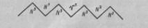
“екст 1.2. ѕрочитайте текст. —кажите, что вы узнали о: a) resistor; б) zigzag pattern; в) capacitance. ѕрочитайте текст еще раз. ќзаглавьте его.
A typical thin-film resistor consists of a fine metal line only a few thousandths of an inch wide and long enough to provide the desired value of resistance. If high precision is required laser trimming is used. If high values are desired, the line can be laid down in a zigzag pattern. To form a capacitance one can lay down a thin film of insulating material between two thin films of metal.

