


We implement the architecture of the neurosynaptic core
using asynchronous QDI circuits that are synchronized with
the global timestep. In this section we describe the concurrent
processes of our architecture using Communicating
Hardware Processes (CHP - see Appendix) that can be
synthesized into QDI asynchronous circuits using MartinТs
synthesis method [9].
A. Scheduler

Fig. 2. Internal structure of the Scheduler. The overall function is: (1)
Receive input packets; (2) Add the stored axonal delay to the time field
of the packet to get the spike delivery time; (3) Demultiplex the address
field of the packet; and (4) Deliver the spike to the appropriate axons at
the edge of a global clock when the global timestep equals the computed
delivery time of the spikes.
The scheduler receives packets from outside the core and
delivers spikes on the axons at specific times. The packets
may come from spiking neurons in the core or from outside
the core. In addition to these packets, the scheduler also
receives a clock and a global counter time. The block also
stores a configurable axonal delay (inside an SRAM array)
for each of the axons. Each packet (y) coming in contains
an axon address (y.dest addr) and a time of spike (y.dt -
in units of clock ticks). The scheduler decodes the packet
to determine where the spike should be delivered (the axon
number). The time in the packet is added to the axonal delay
for the specified axon, and this value is compared against
the current global counter time on every tick of a clock that
the scheduler receives. When the time matches, a spike is
delivered to the crossbar. This makes the spike delivery to
the crossbar synchronous with the global system clock. The
CHP of the processs is:

The scheduler implements the axonal delay stored in a
1024 (number of axons) by 4 (range of delays) SRAM
array. It receives the packet in the channel IN, adds the
axonal delay to the time in the packet, waits for the global
time to reach this value and then delivers the spike to the
axon corresponding to the address in the packet. Besides
implementing the axonal delay, this procedure synchronizes
input spikes to the core with the clock edge, implementing
the first of the two phases of operation (Section II-C) that
allow the system to produce 1-1 correspondence with a
software simulator.
The internal blocks of the scheduler are illustrated in Fig.
2. For our prototype chip, we used a common delay block
instead of a full 1024 „ 4 SRAM array to implement the
axonal delay. This fixed delay is a 4 bit number that can be
configured at the chipТs startup, and is the delay value for all
axons. The Adder adds this delay to the time value in the
packet and passes it to the DEMUX/DECODE unit. The
control for the DEMUX/DECODE unit is the destination
address in the input packet, slack-matched to the SRAM
and the adder. The DEMUX then outputs 5 bits indicating
|
|
|
the final timestamp for spike release to the axon. This value
goes to 1 of 1024 [Delay + Sync] blocks. These blocks must
contain full buffers at the input because all the hardware
used prior to this stage is time-shared and the DEMUX
output channel has to be УreleasedФ as soon as possible
to allow assertion of the next spike. Each [Delay + Sync]
unit compares the timestamp of the global timer with the
obtained final timestamp and initiates a spikes to an axon
when the value matches.
The clock synchronization is contained in the [Delay
+ Sync] unit. The synchronization part is not trivial and
requires some design effort. The data obtained from the
DEMUX/DECODE must be aligned to the clock without
any knowledge of the data arrival time in relationship to
the clock edge. Precautions have to be taken in order to
avoid potential metastability during synchronization with the
global clock. Such metastbility may occur since there is no
timing correlation between the edge of the global clock and
the packets arriving from the router. A modified two flip-flop
synchronization scheme is used in our design [10].
B. Axon Token-Ring
At an edge of the synchronizing clock, the scheduler
pulls up the axon lines that have spikes. Each axon has
a corresponding row (a wordline) in the crossbar memory
array. The dendrites (inputs) of a neuron correspond to a
column (bit line) of the crossbar array. Since a dendrite
can potentially connect to multiple axons, the rows of the
crossbar have to be asserted in a mutually exclusive manner.
This function is carried out by an array of axon servers that
implement a token-ring mutual exclusion algorithm [11].
Each server has an axon as its input and the wordline of the
crossbar as its output. A token circulates among the servers
to give them mutually exclusive access to the crossbar.
When an axon is asserted, its server requests its neighbor
to pass the token. The request propagates through the
token-ring, and the token is passed along to the requesting
server. Upon the arrival of the token, the server asserts the
corresponding row of the crossbar. The CHP of an individual
server is given below. Channel A communicates with the
axon from the scheduler and channel WL with the crossbar,
while channels U and D communicate with the neighbor
above or below. The local variable b represents the token.
The D port of the last server is connected to the U port of the
first server. The channel C communicates with a completion
tree (see Fig. 1) that indicates when all the neurons have
completed processing events for a particular axon.
C. Crossbar Memory
The states of the memory cells of the crossbar array
represent the synaptic configuration of a network (i.e.
which axons connect to which neurons) and determine the
unique properties of that particular network. Organizing the
synapses in this crossbar structure allows an active axon
to fan out to potentially 256 neurons in parallel through a
single control operation. For large connectivity, this reduces
the dynamic power consumption and accelerates the speed
at which the network is updated.
The configuration of the crossbar has to be set up prior
to the operation time of the chip. We included shift register
scanners to configure the bit cells of the array. Standard 6T
|
|
|
SRAM cells were used as the bit cells. The axon token-ring
controls the wordlines of the bit cells while a set of synapse
controllers interfaces the bitlines with the neurons. The CHP
of a synapse controller unit is given below.

When the axon token-ring drives one of the wordlines
of the crossbar, one of the two bitlines of each cell in
the corresponding row will discharge asserting either the
BL.t or the BL.f wires of the synapse controller. If BL.t
is asserted the controller communicates with the neuron
corresponding to the column to update the neuronТs state.
Once this communication is over, or if BL.f was the
wire originally asserted, the controller communicates with
a completion tree. The right-most controller receives the
ФtypeФ information for each axon (they are stored in the
last 2 bit cells of each crossbar row) and communicates
this information to the neurons. Once all synapse controllers
have completed their operation, the completion tree
communicates wih the C channel of the axon token-ring,
after which the token-ring unit with the token releases the
wordline of the crossbar and token becomes free to travel.
Another token-ring unit with an active axon will then get
the token and assert its corresponding wordline.
D. Neuron
The neurons are the basic computational units in the
system. They were implemented using dedicated circuits
(non-multiplexed), allowing all the neural updates to happen
in parallel. This parallelism comes at the cost of relative
density inefficiency that is in part mitigated by our use of a
dense technology.
The design of the neuron circuits needs to accomodate two
conflicting requirements. On the one hand, a neuron must
service events quickly to avoid holding up the crossbar. On
the other hand, a neuron receives very few events in typical
scenarios, so it must not burn dynamic power when it is idle.
A purely event-driven design is therefore ideal: it has a fast
service time (100MHz-GHz range), but only burns power
during the rare occurrence of an event.
During the first phase of operation (Section. II-C) each
neuron receives event-driven synaptic input from the crossbar
memory synapse controller. The neurons update their
state (represented by an internal voltage V) by integrating
the incoming synapses (Section. II-A). During the second
phase of operation, the neurons synchronize with the global
clock edge, at which point they output a spike (represented
by a 1 bit output) if their voltage is above threshold or leak
out an amount of the voltage if it is below threshold. The
synchronization of the neuron during the second phase of
operation, along with the synchronization of the scheduler
during the first phase (Section. III-A) ensures that the operation
in the core is in 1-1 correspondence with a software
simulator.
The internal parameters of the neurons (the threshold,
the leak, and the three synaptic strengths) are configured
at start-up. They are all represented with 8-bit integers in
2Тs compliment form. The internal voltage of a neuron is
represented by a 10-bit integer also in 2Тs compliment form.
The operation of the neuron is decomposed into control
and datapath blocks. A block diagram of the processes
involved is illustrated in Fig. 3.
!

Fig. 3. Block diagram of the neuron. The control block interfaces with
the crossbar, directs information flow in the datapath, synchronizes with
the global time step and outputs a spike when the neuron voltage exceeds
its threshold. The datapath elements update the voltage after each synaptic
event and check for a spike when directed by the control.
The CHP of the control block is:

The control block interfaces with the synaptic input coming
from the neuronТs dedicated crossbar column through
the channel N. Upon a communication request on this
|
|
|
channel, the control reads in the ФtypeФ information of the
axon through the channel G that connects to the synapse
controller representing the last two columns of the crossbar.
Before completing the handshake in N the control communicates
with the datapath of the neuron through channelsM5
(that relays synaptic type information) and M2 (for voltage
control in the datapath). Once these communication actions
have completed N and G are acknowledged and the next
cycle of synaptic inputs may come in.
In the second half of the global timestep, the neurons
receive a synchronization event in the channel C (that is
driven by a process that uses one of the edges of the
global clock to initiate a handshake). When this event comes
in, the control initiates a communication with the datapath
through the T channel. The datapath sends back one of three
distinct values indicating whether the voltage for the current
timestep is above threshold, below threshold but above zero;
or below zero. If the voltage is above threshold the control
communicates with the AER transmitter through the channel
S to send out a spike. Through M2 the control also instructs
the datapath to reset the voltage to 0 if there is a spike or
if the voltage is below 0. If the voltage has not been reset
to 0, the control instructs the datapath to apply the leak to
the current voltage.
The CHP of the datapath units are:

When the control drives MERGE 5, the process forwards
either a synaptic strength (during the integration
phase), a leak (during the resetting phase if V > 0) or
the value 0 (during the resetting phase if V <= 0) to
one of the inputs of the ADDER process. When the
control drives MERGE 2, the process forwards either the
previous voltage (during integration) or the value 0 (if
V > threshold or V < 0 during the firing phase) to
the other input of ADDER. The ADDER process is a
10 bit adder that sends out the sum of its inputs to the
COMPARATOR and the MERGE 2 processes when
they request it. The control drives COMPARATOR when
it needs to evaluate the state of the neuron voltage.
E. AER transmitter
Spikes from the 2-dimensional array of neurons are sent
out of the core through token-ring AER transmitter circuits
[8] that allow all the neurons to share one output channel.
In this scheme, a set of row servers and column servers
circulate tokens in each dimension of the neuron array
and give spiking neurons mutually exclusive access to the
shared communication channel. A counter keeps track of the
location of the tokens, and sends out neuron addresses upon
request. This methodology leads to compact transmitter
circuits capable of efficiently servicing clusters of spiking
activity.
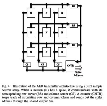
Fig. 4. Illustration of the AER transmitter architecture using a 3„3 sample
neuron array. When a neuron (N) has a spike, it communicates with its
corresponding row server (RS) and column server (CS). A counter (CNTR)
keeps track of circulating row and column tokens and sends out the spike
address through the shared output bus.
The design of the transmitter is illustrated in Fig 4. The
sequence of operation is: (1) A spiking neuron asserts a
row request line; (2) The corresponding row server requests
for the row token from its neighbors; (3) As the row token
moves, the counter keeps track of its position; (4) Upon
receipt of the token, the row server acknowledges the row
request; (5) The neuron then asserts a column request line;
(6) The corresponding column server requests the column
|
|
|
token from its neighbors; (7) As the column token moves,
the counter keeps track of its position; (8) Upon receipt of
the token the column server communicates with the counter
to send out the row and column token addresses and then
acknowledges the column request; (9) The neuron does a
second communication with the row server to indicate the
completion of service.
The neurons interface with their respective servers via
open-drain shared row request lines and shared column
request lines. The servers also communicate with the counter
via shared wires. These wires need to be carefully implemented
since transitions are shared across processes and
span an entire dimension of the neuron array.
IV. RESULTS
The neurosynaptic core was fabricated using IBMТs 45nm
SOI process and occupied 4.2mm2 of silicon (Fig. 5, left).
Each of the 256 neurons in the core occupies 35μm „ 95μm.
Each SRAM bitcell in the 1024 „ 256 synaptic crossbar
array occupied 1.3μm2 (plus another 1.9 μm2 associated
with conservatively-designed periphery). A custom printed
circuit board allows the chip to interface with a PC through
a USB link (Fig. 5, right).
membrane potential is above threshold, and if so, it produces a
spike and resets the membrane potential to 0; these spikes are
encoded and sent off as address events in a sequential fashion.
After checking for a spike, the leak is applied.
The purpose of breaking neural updates into two phases
is to ensure that the hardware and software are always in
lock step at the end of each time step. Specifically, the order
in which address events arrive to the core or exit the core
can vary from chip to chip due to resource arbitrationЧ
especially when events are sent through a non-deterministic
routing network. To remain one-to-one, the different orderings
must not influence the spiking dynamics. We achieve one-toone
equivalence by first accounting for all the axon inputs,
and then checking for spikes after these inputs have been
processed. This also gives us a precise bound for operating in
real time: all address events must be accounted for before the
synchronization event, which we trigger once per millisecond.
IV. TEST RESULTS
2mm
Fig. 3. (left) Neurosynaptic die measures 2mm „ 3mm including the IЦO
pads. (right) Test board that interfaces with the chip via a USB 2.0 link. Spike
events are sent to a PC for data collection, and are also routed back to the
chip to implement recurrent connectivity.
We have designed, fabricated, and tested our neurosynaptic
core using IBMТs 45nm SOI process. Our core has 3.8 million
transistors in 4.2mm2 of silicon (Fig. 3, left), and all transistors
are ultra-high threshold (UVT) to reduce leakage.
The coreТs 256 neurons are organized into a 16 „ 16 array,
where each neuron occupies 35μm „ 95μm. For crossbar
synapses, we use a custom SRAM array with 1024„256 bits
implementing over 256K binary synapses. The bitcell occupies
1.3μm2 (plus another 1.9μm2 associated with conservativelydesigned
periphery). Because our bitcell was custom, its area
is approximately 4„ larger than the commercially available
bitcells in the same technology.
To test our design, we built a custom printed circuit board
that interfaces with a PC through a USB link (Fig. 3, right).
Through this link, we can interface our chip to virtual and
real environments via address event communication, as well
as configure neuronЦsynapse parameters via a shift-register
scanner (not shown).
For testing, we focused on active power1 and one-to-one
equivalence with software. We also demonstrate that our chip
can implement a well-known neural algorithm, a restricted
Boltzmann machine (RBM), which acts as a front end to an
off chip linear classifier for recognizing digits.
1Active power is our primary focus because passive power depends on the
fabrication options, and can be addressed by process selection and availability.
A. Active Power
In our chip, active power scales linearly with spike activity
since the design is purely event driven. To measure active
power, we measure the increase in current beyond the baseline
during high activity (averaged), where all neurons and axons
are active in each time step (1kHz rate).2 Our measurements
are repeated over a range of supply voltages (Fig. 4); at Vdd =
0.85V, the core consumes just 45pJ/spike.
0.85 0.9 0.95 1 1.05
V
core
(V)
Active Energy per Spike (pJ)
0.85 0.9 0.95 1 1.05
10−2
V
core
(V)
Passive Power (W)
|
|
|
Fig. 4. Active energy per spike (red) decreases approximately linearly with
lower Vdd, whereas the coreТs total passive power (blue, inset) decreases
exponentially, shown on a log scale.
B. One-to-One Equivalence
To test that the chip satisfied one-to-one equivalence, we
configured the synaptic strength and leak values of each
neuron to +1, and the thresholds to +100. Then, we generated
a pseudorandom connectivity where each synapse had a 20%
probability of being 1. Lastly, the CPLD was set to route all
neuron spikes back into the core (neuron 0,1,2 drove axon
0,1,2, respectively), creating a complex recurrent network.
Running the chip we observe that after 100 time steps, all
the neurons spike in unison due to their identical positive
leaks. This first barrage of spikes is routed back around to the
axonal inputs, activating a pseudorandom pattern of excitatory
recurrent connections; these inputs cause neurons to spike
earlier in the next cycle, thereby having a de-synchronizing
effect. Within a few cycles, the recurrently-driven activity
dominates the dynamics leading to a complex spatiotemporal
pattern. We simulated a software network with an identical
configuration, and confirmed that the software and hardware
have identical behavior (Fig. 5).
C. Implementing a Restricted Boltzmann Machine (RBM)
Our neurosynaptic core is capable of implementing a
wide range of neural network algorithms, where weights are
first learned offline, and then transformed into a hardwarecompatible
format. We present one example that implements
a RBM, which is a well-known algorithm for classification and
inference tasks. Specifically, we trained a two-layer RBM with
484 visible units and 256 hidden units on handwritten digits
from the MNIST dataset. Our learning procedure followed
directly from [5]; briefly, we use contrastive divergence to
learn 484„256 real-valued weights to capture the probability
2Note that an axon event contributes less active power than a spike.

Fig. 5. Left: Neurosynaptic die measures 2mm „ 3 mm including the I-O
pads. Right: Test board that interfaces with the chip via a USB 2.0 link.
Spike events are sent to a PC for data collection and can also be routed
back to the chip via the CPLD.
A. Active Power
Our primary focus during the design was the reduction of
active power since passive power can be addressed through
fabrication options and active leakage reduction circuitry
[13]. The purely event-driven nature of the core allowed
us to achieve an ultra-low-power design where active power
is dependent only on the activity rate of the neurons. Our
QDI methodology allows us to readily reduce the operating
voltage in the core without affecting the correctness of the
neural algorithms that it is running. We discuss the power
consumption of the chip in Ref. [14]. At Vdd = 0.85, the
core consumes just 45pJ/spike.
B. Example Application
The neurosynaptic core produces one-to-one equivalence
with models in software neural simulators making it convenient
to set up neural algorithms on the chip. A wide range
of traditional artificial neural network algorithms [15] for
various applications can readily be configured. In addition,
the biologically-grounded neuron models in our chip allow
novel bio-inspired approaches to be implemented for solving
engineering problems. For example, individual neurons in
the core can efficiently implement a common processing
technique in biological neural pathwaysЧcoincidence
detectionЧthat does not have an analog [16] in the computational
units of traditional artificial neural networks. In Fig.
6 we illustrate a bio-inspired sound-localization method in
our chip using this technique.
V. CONCLUSION
We have demonstrated a compact modular architecture
that can be a building block for large-scale neuromorphic
systems. Our asynchronous neurosynaptic core combines
digital neurons, large synaptic fanout, and address-event
communication circuits in a low-power event-drive fabric.
The embedded crossbar array allows us to implement
synaptic fanout without resorting to off-chip memory that
can create I-O bottlenecks. The asynchronous quasi-delayinsensitive
circuits that we used led to robust circuits
that are operational across a wide range of voltages and
temperatures, making the neurosynaptic core ideally suited
for mobile applications. Our implementation methodology
guaranteed that there is strict correspondence between the
neural algorithm running on the core and an equivalent
simulation of it in a software simulator, greatly increasing
the usability of the chip and its deployment in real-world
scenarios.
APPENDIX
The CHP notation we use is based on HoareТs CSP [17]. A full
description of CHP and its semantics can be found in [9]. What
follows is a short and informal description.
Х Assignment: a:= b. This statement means Уassign the value
of b to a.Ф We also write a↑ for a:= true, and a↓ for
a:= false.
Х Selection: [G1 → S1 []... [] Gn → Sn], where GiТs
are boolean expressions (guards) and SiТs are program parts.
The execution of this command corresponds to waiting until
one of the guards is true, and then executing one of the
statements with a true guard. The notation [G] is shorthand
for [G → skip], and denotes waiting for the predicate
G to become true. If the guards are not mutually exclusive,
we use the vertical bar У|Ф instead of У[].Ф
Х Repetition: *[G1 → S1 []... [] Gn → Sn]. The execution
of this command corresponds to choosing one of the true
guards and executing the corresponding statement, repeating
this until all guards evaluate to false. The notation *[S] is
short-hand for *[true → S].
Х Send: X!e means send the value of e over channel X.
Х Receive: Y?v means receive a value over channel Y and
store it in variable v.
Х Probe: The boolean expression X is true iff a communication
over channel X can complete without suspending.
Х Sequential Composition: S;T
Х Parallel Composition: S T or S,T.
 Fig. 6. Sound localization using axonal delays and coincidence detection. Coincidence detecting neurons spike when their inputs come within a time
window defined by the neuronsТ internal parameters. Left: There is a difference in the arrival times of a sound in two sensors located at opposite sides
of a system (e.g. two ears). Hence the sensors contain information about the location of the sound source. This information is decoded by a set of
coincidence-detecting neurons (circles) arranged systemically along axonal delay lines. For example, the top-most neuron has a short delay line from
the left sensor but a long delay line from the right sensor. When the sound source is exactly adjacent to the right sensor, the axonal delay in the right
sensor path compensates for the time lag between the arrival of the sound in the two sensors. The neuron would thus receive coincident inputs and
respond maximally, decoding the location of the sound source. Avian auditory pathways use this mechanism for sound localization [12]. Center: The
neurosynaptic core can use a similar method for localizing a sound source based on the inputs of two sensors (not shown). The sensors would have to
receive the sound and convert them into address-event packets. The first input (corresponding to the sensor closer to the sound source) will hit several
axon lines that implement different axonal delays using the scheduler (in our prototype system, the operation of the scheduler is replicated outside the
chip). Each neuron in the core will connect to one of these axon lines. The second input will hit a separate axon line that connects to all neurons.
Those neurons that have temporally coincident inputs will spike maximally, representing the location of the sound source in neural space. The difference
between the input arrival times in the two sensors will typically be in the 10s of microseconds range. The sensors may amplify this difference to keep
the core at its usual (millisecond) precision range, or the time step in the core may be made more precise. Right: The dynamics of the chip when the
axon lines are driven in the manner suggested. The sound source starts at the left of the core, moving all the way to the right in a semi-circular trajectory,
and then back to its original position. As the source moves, a unique neuron spikes to indicate the new location. A total of 50 neurons were included
to identify 50 distinct positions. A software simulation running the same algorithm confirms that our chip is in 1-1 correspondence.
ACKNOWLEDGMENTS
This research was sponsored by DARPA under contract No.
HR0011-09-C-0002. The views and conclusions contained herein
are those of the authors and should not be interpreted as representing
the official policies, either expressed or implied, of DARPA or
the U.S. Government. Authors thank William Risk and Sue Gilson
for project management, Ben Hill, Ben Johnson, Rob Karmazin,
Carlos Otero, Jon Tse, Scott Fairbanks, Scott Hall, Kavita Prasad
for physical design, Steven Esser and Greg Corrado for their work
on digital neurons, and Andrew Cassidy and Rodrigo Alvarez for
developing software for data collection.
REFERENCES
[1] E. R. Kandel, J. H. Schwartz, and T. M. Jessell, Principles of Neural
Science. McGraw-Hill Medical, 4th ed., July 2000.
[2] R. Ananthanarayanan, S. K. Esser, H. D. Simon, and D. S. Modha,
УThe cat is out of the bag: cortical simulations with 109 neurons, 1013
synapses,Ф in Proceedings of the Conference on High Performance
Computing Networking, Storage and Analysis, SC Т09, (New York,
NY, USA), pp. 63:1Ц63:12, ACM, 2009.
[3] C. Mead, УNeuromorphic electronic systems,Ф Proceedings of the
IEEE, vol. 78, pp. 1629 Ц1636, Oct. 1990.
[4] K. Boahen, УNeurogrid: emulating a million neurons in the cortex,Ф
IEEE international conference of the engineering in medicine and
biology society, 2006.
[5] P. Dayan and L. F. Abbott, Theoretical Neuroscience: Computational
and Mathematical Modeling of Neural Systems. The MIT Press, 2005.
[6] A. J. Martin, УProgramming in VLSI: From communicating processes
to delay-insensitive circuits,Ф in Developments in Concurrency and
Communication, UT Year of Programming Series (C. A. R. Hoare,
ed.), pp. 1Ц64, Addison-Wesley, 1990.
[7] M. A. Mahowald, VLSI analogs of neuronal visual processing: a
synthesis of form and function. PhD thesis, Pasadena, CA, USA,
1992. UMI Order No. GAX92-32201.
[8] N. Imam and R. Manohar, УAddress-event communication using
token-ring mutual exclusion,Ф in ASYNC, pp. 99Ц108, IEEE Computer
Society, 2011.
[9] A. J. Martin, УProgramming in VLSI: From communicating processes
to delay-insensitive circuits,Ф in Developments in Concurrency and
Communication, UT Year of Programming Series (C. A. R. Hoare,
ed.), pp. 1Ц64, Addison-Wesley, 1990.
[10] F. Akopyan, Hybrid Synchronous/Asynchronous Design. Ph.D. thesis,
Cornell University, April 2011.
[11] A. J. Martin, УDistributed mutual exclusion on a ring of processes,Ф
Sci. Comput. Program., vol. 5, pp. 265Ц276, October 1985.
[12] B. Grothe, УNew roles for synaptic inhibition in sound localization,Ф
Nature Reviews Neuroscience, vol. 4, pp. 1Ц11, 2003.
[13] C. T. O. Otero, J. Tse, and R. Manohar, УStatic power reduction techniques
for asynchronous circuits,Ф in IEEE International Symposium
on Asynchronous Circuits and Systems, May 2010.
[14] P. Merolla, J. Arthur, F. Akopyan, N. Imam, R. Manohar, and
D. Modha, УA digital neurosynaptic core using embedded crossbar
memory with 45pJ per spike in 45nm,Ф Proceedings of the IEEE
Custom Integrated Circuits Conference, September 2011.
[15] S. Haykin, Neural Networks and Learning Machines (3rd Edition).
Prentice Hall, 3 ed., Nov. 2008.
[16] W. Maass and C. M. Bishop, eds., Pulsed neural networks. Cambridge,
MA, USA: MIT Press, 1999.
[17] C. A. R. Hoare, УCommunicating sequential processes,Ф Communications
of the ACM, vol. 21, no. 8, pp. 666Ц677, 1978.
| ќ. ». ‘ед€ев, ƒ. ѕ. ѕауков Ќейронные сети: прогнозирование как задача распознавани€ образов |
¬ведение
¬рем€ - это одно из самых интересных пон€тий, которые интересуют человека с ƒревних времен. ѕон€ть и подчинить себе врем€ человечество стремилось всегда, потому что знание будущего дает невиданную силу прин€ти€ решений в различных област€х человеческой де€тельности. ¬опрос определени€ будущего был и остаетс€ актуальным по сегодн€шний день. Ѕольшой интерес представл€ют задачи прогнозировани€ погоды по результатам соответствующих атмосферных измерений, селекционировани€ новых видов растений и животных, определений возможностей индивидуумов в определенных област€х с помощью соответствующей системы контрольных тестов и т.д. ќсобо важное значение прогнозирование имеет в таких област€х, как индустри€, экономика, коммерци€ (прогнозирование экономических показателей, динамики цен на тот или иной продукт, курса акций на какое-то врем€ вперед и т.д.).
ќднако создать машину времени человек не может, мы знаем, что было в прошлом, но совершенно точно утверждать положение вещей в будущем не дано никому из нас. Ќесмотр€ на это, люди всегда стремились предугадать будущее, примен€€ при этом самые различные способы: в простом народе с давних времен попул€рны народные приметы, математики используют дл€ этого более формальные методы и способы прогнозировани€ - они примен€ют статистические и веро€тностные характеристики, по которым возможно с определенной веро€тностью утверждать, что будущее событие произойдет или нет.
Ќар€ду с традиционными методами прогнозировани€ сегодн€ бурно развиваетс€ теори€ искусственных нейронных сетей, котора€ хорошо зарекомендовала себ€ в области управлени€, там, где необходимо применение человеческого интеллекта, в частности при решении задач прогнозировани€.
Ёто научное направление родилось на стыке таких наук как нейробиологи€, хими€, физика, математика, информатика, философи€, психологи€ и др. интерес к нейронным сет€м был вызван как теоретическими, так и прикладными достижени€ми в этой области. Ќейросети неожиданно открыли возможности использовани€ вычислений в сферах, до этого относ€щихс€ лишь к области человеческого интеллекта, возможности создани€ машин, способность которых учитьс€ и запоминать удивительным образом напоминает мыслительные процессы человека.
»скусственные нейронные сети состо€т из элементов, функциональные возможности которых аналогичны большинству элементарных функций биологического нейрона. Ёти элементы затем организуютс€ по способу, который может соответствовать (или не соответствовать) анатомии мозга. Ќесмотр€ на такое поверхностное сходство, искусственные нейронные сети демонстрируют удивительное число свойств присущих мозгу. Ќапример, они обучаютс€ на основе опыта, обобщают предыдущие прецеденты на новые случаи и извлекают существенные свойства из поступающей информации, содержащей излишние данные.
Ќесмотр€ на такое функциональное сходство, даже самый оптимистичный их защитник не предположит, что в скором будущем искусственные нейронные сети будут дублировать функции человеческого мозга. –еальный "интеллект", демонстрируемый самыми сложными нейронными сет€ми, находитс€ ниже уровн€ дождевого черв€, и энтузиазм должен быть умерен в соответствии с современными реали€ми. ќднако равным образом было бы неверным игнорировать удивительное сходство в функционировании некоторых нейронных сетей с человеческим мозгом. Ёти возможности, как бы они ни были ограничены сегодн€, навод€т на мысль, что глубокое проникновение в человеческий интеллект, а также множество революционных приложений, могут быть не за горами.
»скусственные нейронные сети могут мен€ть свое поведение в зависимости от внешней среды. Ётот фактор в большей степени, чем любой другой, ответствен за тот интерес, который они вызывают. ѕосле предъ€влени€ входных сигналов (возможно, вместе с требуемыми выходами) они самонастраиваютс€, чтобы обеспечивать требуемую реакцию. Ѕыло разработано множество обучающих алгоритмов, каждый со своими сильными и слабыми сторонами. ¬се еще существуют проблемы относительно того, чему нейросеть может обучитьс€ и как обучение должно проводитьс€.
ќтклик сети после обучени€ может быть до некоторой степени нечувствителен к небольшим изменени€м входных сигналов. Ёта внутренне присуща€ способность видеть образ сквозь шум и искажени€ жизненно важна дл€ распознавани€ образов в реальном мире. ќна позвол€ет преодолеть требование строгой точности, предъ€вл€емое обычным компьютером, и открывает путь к системе, котора€ может иметь дело с тем несовершенным миром, в котором мы живем. ¬ажно отметить, что искусственна€ нейронна€ сеть делает обобщени€ автоматически благодар€ своей структуре, а не с помощью использовани€ "человеческого интеллекта" в форме специально написанных компьютерных программ.
Ќекоторые из искусственных нейронных сетей обладают способностью извлекать сущность из входных сигналов. Ќапример, сеть может быть обучена на последовательность искаженных версий буквы "ј". ѕосле соответствующего обучени€ предъ€вление такого искаженного примера приведет к тому, что сеть породит букву совершенной формы. ¬ некотором смысле она научитс€ порождать то, что никогда не видела.
Ёта способность извлекать идеальное из несовершенных входов ставит интересные философские вопросы. ќна напоминает концепцию идеалов, выдвинутую ѕлатоном в его "–еспублике". ¬о вс€ком случае, способность извлекать идеальные прототипы €вл€етс€ у людей весьма ценным качеством.
»скусственные нейронные сети не €вл€ютс€ панацеей. ќни, очевидно, не год€тс€ дл€ выполнени€ таких задач, как начисление заработной платы. ѕохоже, однако, что им будет отдаватьс€ предпочтение в большом классе задач распознавани€ образов, прогнозировани€, создание ассоциативной пам€ти, экономики, управлени€ объектами, с которыми плохо или вообще не справл€ютс€ обычные компьютеры.
ѕостановка задачи
¬ различных област€х человеческой де€тельности часто возникают ситуации, когда по имеющейс€ информации (данным), обозначим ее X, требуетс€ предсказать (спрогнозировать, оценить) некоторую величину Y, стохастически св€занную с X (то есть X и Y имеют некоторое распределение L(X,Y)), но которую непосредственно измерить невозможно (например, Y может относитьс€ к будущему, а X - к насто€щему). “ак, например, может представл€ть интерес прогноз успеваемости первокурсников очередного набора по оценкам, полученным ими на вступительных экзаменах. «десь X - средний балл студентов на вступительных экзаменах, а Y - средний балл по итогам, скажем, первой сессии; при этом совместное распределение X и Y можно в принципе определить (оценить) по аналогичным данным за прошлые годы.
¬ общем случае X означает некоторую совокупность {X1, X2,:} наблюдаемых случайных величин, которые в рассматриваемом контексте называютс€ предсказывающими (или прогнозными) переменными, и задача состоит в построении такой функции ‘(’), которую можно было бы использовать в качестве оценки дл€ прогнозируемой величины Y: ‘(’)=Y (т.е. чтобы она была в каком-то смысле близка к Y); такие функции ‘(’) называют предикторами величины Y по X. –азработка методов построени€ оптимальных (в том или ином смысле) предикторов и составл€ет главную задачу прогнозировани€.
≈сли совокупность величин {X1, X2,:, Xn} представл€ет собой значени€ какого-либо параметра, измен€ющегос€ во времени, то такую совокупность называют временным р€дом, при этом каждое значение соответствует значению параметра в конкретное врем€ t1, t2,:,tn. «адача прогнозировани€ в этом случае заключаетс€ в определении значени€ измер€емой величины X в момент времени tn+1, tn+2, tn+3,:, то есть дл€ выполнени€ прогнозировани€ необходимо вы€вить закономерность этого временного р€да.
–азличают многошаговый и одношаговый прогноз.
ћногошаговым прогнозом называют долгосрочный прогноз, цель которого состоит в определении основного тренда, дл€ некоторого фиксированного промежутка времени в будущем. ѕри этом прогнозирующа€ система (в нашем случае - нейронна€ сеть) использует полученные прогнозные значени€ временного р€да дл€ выполнени€ дальнейшего прогноза, то есть использует их как входные данные.
ќдношаговым прогнозированием называют краткосрочный прогноз (на один шаг), при этом дл€ получени€ прогнозированной величины используют только фактические данные. ясно, что одношаговое прогнозирование более точно, но оно не позвол€ет выполн€ть долгосрочные прогнозы.
Ѕиологический прототип нейрона
–азвитие искусственных нейронных сетей вдохновл€етс€ биологией, то есть, рассматрива€ сетевые конфигурации и алгоритмы, исследователи мысл€т их в терминах организации мозговой де€тельности. Ќо на этом аналоги€ может и закончитьс€. Ќаши знани€ о работе мозга ограничены. ѕоэтому разработчикам сетей приходитс€ выходить за пределы современных биологических знаний в поисках структур, способных выполн€ть полезные функции. ¬о многих случа€х это приводит к необходимости отказа от биологического правдоподоби€, мозг становитс€ просто метафорой, и создаютс€ сети, невозможные в живой материи или требующие неправдоподобно больших допущений об анатомии и функционировании мозга.
Ќесмотр€ на то, что св€зь с биологией слаба и зачастую несущественна, искусственные нейронные сети продолжают сравниватьс€ с мозгом. »х функционирование часто напоминает человеческое познание, поэтому трудно избежать этой аналогии. сожалению, такие сравнени€ неплодотворны и создают неоправданные ожидани€, неизбежно ведущие к разочарованию.
Ќесмотр€ на сделанные предупреждени€, полезно все же знать кое-что о нервной системе млекопитающих, так как она успешно решает задачи, к выполнению которых лишь стрем€тс€ искусственные системы. Ќервна€ система человека, построенна€ из элементов, называемых нейронами, имеет ошеломл€ющую сложность. ќколо 1011 нейронов участвуют в примерно 1015 передающих св€з€х, имеющих длину метр и более. аждый нейрон обладает многими качествами, общими с другими элементами тела, но его уникальной способностью €вл€етс€ прием, обработка и передача электрохимических сигналов по нервным пут€м, которые образуют коммуникационную систему мозга.
 –исунок 1 - Ѕиологический нейрон
Ќа рисунке 1 показана структура пары типичных биологических нейронов. ƒендриты идут от тела нервной клетки к другим нейронам, где они принимают сигналы в точках соединени€, называемых синапсами. ѕрин€тые синапсом входные сигналы подвод€тс€ к телу нейрона. «десь они суммируютс€, причем одни входы стрем€тс€ возбудить нейрон, другие - воспреп€тствовать его возбуждению. огда суммарное возбуждение в теле нейрона превышает некоторый порог, нейрон возбуждаетс€, посыла€ по аксону сигнал другим нейронам. ” этой основной функциональной схемы много усложнений и исключений, тем не менее большинство искусственных нейронных сетей моделируют лишь эти простые свойства.
»скусственный нейрон
»скусственный нейрон имитирует в первом приближении свойства биологического нейрона. Ќа вход искусственного нейрона поступает некоторое множество сигналов, каждый из которых €вл€етс€ выходом другого нейрона. аждый вход умножаетс€ на соответствующий вес, аналогичный синаптической силе, и все произведени€ суммируютс€, определ€€ уровень активации нейрона. Ќа рисунке 2 представлена модель, реализующа€ эту идею. ’от€ сетевые парадигмы весьма разнообразны, в основе почти всех их лежит эта конфигураци€. «десь множество входных сигналов, обозначенных x1, x2,:, xn, поступает на искусственный нейрон. Ёти входные сигналы, в совокупности, обозначаемые вектором X, соответствуют сигналам, приход€щим в синапсы биологического нейрона. аждый сигнал умножаетс€ на соответствующий вес w1, w2,:, wn, и поступает на суммирующий блок, обозначенный Σ. аждый вес соответствует <силе> одной биологической синаптической св€зи. (ћножество весов в совокупности обозначаетс€ вектором W.) —уммирующий блок, соответствующий телу биологического элемента, складывает взвешенные входы алгебраически, создава€ выход, который мы будем называть NET. ¬ векторных обозначени€х это может быть компактно записано следующим образом: NET = XW.
–исунок 1 - Ѕиологический нейрон
Ќа рисунке 1 показана структура пары типичных биологических нейронов. ƒендриты идут от тела нервной клетки к другим нейронам, где они принимают сигналы в точках соединени€, называемых синапсами. ѕрин€тые синапсом входные сигналы подвод€тс€ к телу нейрона. «десь они суммируютс€, причем одни входы стрем€тс€ возбудить нейрон, другие - воспреп€тствовать его возбуждению. огда суммарное возбуждение в теле нейрона превышает некоторый порог, нейрон возбуждаетс€, посыла€ по аксону сигнал другим нейронам. ” этой основной функциональной схемы много усложнений и исключений, тем не менее большинство искусственных нейронных сетей моделируют лишь эти простые свойства.
»скусственный нейрон
»скусственный нейрон имитирует в первом приближении свойства биологического нейрона. Ќа вход искусственного нейрона поступает некоторое множество сигналов, каждый из которых €вл€етс€ выходом другого нейрона. аждый вход умножаетс€ на соответствующий вес, аналогичный синаптической силе, и все произведени€ суммируютс€, определ€€ уровень активации нейрона. Ќа рисунке 2 представлена модель, реализующа€ эту идею. ’от€ сетевые парадигмы весьма разнообразны, в основе почти всех их лежит эта конфигураци€. «десь множество входных сигналов, обозначенных x1, x2,:, xn, поступает на искусственный нейрон. Ёти входные сигналы, в совокупности, обозначаемые вектором X, соответствуют сигналам, приход€щим в синапсы биологического нейрона. аждый сигнал умножаетс€ на соответствующий вес w1, w2,:, wn, и поступает на суммирующий блок, обозначенный Σ. аждый вес соответствует <силе> одной биологической синаптической св€зи. (ћножество весов в совокупности обозначаетс€ вектором W.) —уммирующий блок, соответствующий телу биологического элемента, складывает взвешенные входы алгебраически, создава€ выход, который мы будем называть NET. ¬ векторных обозначени€х это может быть компактно записано следующим образом: NET = XW.
 –исунок 2 - »скусственный нейрон
—игнал NET далее, как правило, преобразуетс€ активационной функцией F и дает выходной нейронный сигнал OUT. јктивационна€ функци€ может быть обычной линейной функцией OUT = K*NET, где - посто€нна€, пороговой функции, или же функцией, более точно моделирующей нелинейную передаточную характеристику биологического нейрона и представл€ющей нейронной сети большие возможности.
–исунок 2 - »скусственный нейрон
—игнал NET далее, как правило, преобразуетс€ активационной функцией F и дает выходной нейронный сигнал OUT. јктивационна€ функци€ может быть обычной линейной функцией OUT = K*NET, где - посто€нна€, пороговой функции, или же функцией, более точно моделирующей нелинейную передаточную характеристику биологического нейрона и представл€ющей нейронной сети большие возможности.
 –исунок 3 - »скусственный нейрон с активационной функцией
Ќа рисунке 3 блок, обозначенный F, принимает сигнал NET и выдает сигнал OUT. ≈сли блок F сужает диапазон изменени€ величины NET так, что при любых значени€х NET значени€ OUT принадлежат некоторому конечному интервалу, то F называетс€ (сжимающей) функцией. ¬ качестве (сжимающей) функции часто используетс€ логистическа€ или сигмоидальна€ (S-образна€) функци€. Ёта функци€ математически выражаетс€ как F(x) = 1/(1 + е-x). “аким образом,
–исунок 3 - »скусственный нейрон с активационной функцией
Ќа рисунке 3 блок, обозначенный F, принимает сигнал NET и выдает сигнал OUT. ≈сли блок F сужает диапазон изменени€ величины NET так, что при любых значени€х NET значени€ OUT принадлежат некоторому конечному интервалу, то F называетс€ (сжимающей) функцией. ¬ качестве (сжимающей) функции часто используетс€ логистическа€ или сигмоидальна€ (S-образна€) функци€. Ёта функци€ математически выражаетс€ как F(x) = 1/(1 + е-x). “аким образом,
 ѕо аналогии с электронными системами активационную функцию можно считать нелинейной усилительной характеристикой искусственного нейрона. оэффициент усилени€ вычисл€етс€ как отношение приращени€ величины OUT к вызвавшему его небольшому приращению величины NET. ќн выражаетс€ наклоном кривой при определенном уровне возбуждени€ и измен€етс€ от малых значений при больших отрицательных возбуждени€х (крива€ почти горизонтальна) до максимального значени€ при нулевом возбуждении и снова уменьшаетс€, когда возбуждение становитс€ большим положительным. √россберг (1973) обнаружил, что подобна€ нелинейна€ характеристика решает поставленную им дилемму шумового насыщени€. аким образом одна и та же сеть может обрабатывать как слабые, так и сильные сигналы? —лабые сигналы нуждаютс€ в большом сетевом усилении, чтобы дать пригодный к использованию выходной сигнал. ќднако усилительные каскады с большими коэффициентами усилени€ могут привести к насыщению выхода шумами усилителей (случайными флуктуаци€ми), которые присутствуют в любой физически реализованной сети. —ильные входные сигналы в свою очередь также будут приводить к насыщению усилительных каскадов, исключа€ возможность полезного использовани€ выхода. ÷ентральна€ область логистической функции, имеюща€ большой коэффициент усилени€, решает проблему обработки слабых сигналов, в то врем€ как области с падающим усилением на положительном и отрицательном концах подход€т дл€ больших возбуждений. “аким образом, нейрон функционирует с большим усилением в широком диапазоне уровн€ входного сигнала.
–ассмотренна€ проста€ модель искусственного нейрона игнорирует многие свойства своего биологического двойника. Ќапример, она не принимает во внимание задержки во времени, которые воздействуют на динамику системы. ¬ходные сигналы сразу же порождают выходной сигнал. », что более важно, она не учитывает воздействий функции частотной модул€ции или синхронизирующей функции биологического нейрона, которые р€д исследователей считают решающими.
Ќесмотр€ на эти ограничени€, сети, построенные из этих нейронов, обнаруживают свойства, сильно напоминающие биологическую систему. “олько врем€ и исследовани€ смогут ответить на вопрос, €вл€ютс€ ли подобные совпадени€ случайными или следствием того, что в модели верно схвачены важнейшие черты биологического нейрона.
ћногослойные нейронные сети
’от€ один нейрон и способен выполн€ть простейшие процедуры распознавани€, сила нейронных вычислений проистекает от соединений нейронов в сет€х.
рупные и сложные нейронные сети обладают, как правило, большими вычислительными возможност€ми. ’от€ созданы сети всех конфигураций, какие только можно себе представить, послойна€ организаци€ нейронов копирует слоистые структуры определенных отделов мозга. ќказалось, что такие многослойные сети обладают большими возможност€ми, чем однослойные, и в последние годы были разработаны алгоритмы дл€ их обучени€.
ѕо аналогии с электронными системами активационную функцию можно считать нелинейной усилительной характеристикой искусственного нейрона. оэффициент усилени€ вычисл€етс€ как отношение приращени€ величины OUT к вызвавшему его небольшому приращению величины NET. ќн выражаетс€ наклоном кривой при определенном уровне возбуждени€ и измен€етс€ от малых значений при больших отрицательных возбуждени€х (крива€ почти горизонтальна) до максимального значени€ при нулевом возбуждении и снова уменьшаетс€, когда возбуждение становитс€ большим положительным. √россберг (1973) обнаружил, что подобна€ нелинейна€ характеристика решает поставленную им дилемму шумового насыщени€. аким образом одна и та же сеть может обрабатывать как слабые, так и сильные сигналы? —лабые сигналы нуждаютс€ в большом сетевом усилении, чтобы дать пригодный к использованию выходной сигнал. ќднако усилительные каскады с большими коэффициентами усилени€ могут привести к насыщению выхода шумами усилителей (случайными флуктуаци€ми), которые присутствуют в любой физически реализованной сети. —ильные входные сигналы в свою очередь также будут приводить к насыщению усилительных каскадов, исключа€ возможность полезного использовани€ выхода. ÷ентральна€ область логистической функции, имеюща€ большой коэффициент усилени€, решает проблему обработки слабых сигналов, в то врем€ как области с падающим усилением на положительном и отрицательном концах подход€т дл€ больших возбуждений. “аким образом, нейрон функционирует с большим усилением в широком диапазоне уровн€ входного сигнала.
–ассмотренна€ проста€ модель искусственного нейрона игнорирует многие свойства своего биологического двойника. Ќапример, она не принимает во внимание задержки во времени, которые воздействуют на динамику системы. ¬ходные сигналы сразу же порождают выходной сигнал. », что более важно, она не учитывает воздействий функции частотной модул€ции или синхронизирующей функции биологического нейрона, которые р€д исследователей считают решающими.
Ќесмотр€ на эти ограничени€, сети, построенные из этих нейронов, обнаруживают свойства, сильно напоминающие биологическую систему. “олько врем€ и исследовани€ смогут ответить на вопрос, €вл€ютс€ ли подобные совпадени€ случайными или следствием того, что в модели верно схвачены важнейшие черты биологического нейрона.
ћногослойные нейронные сети
’от€ один нейрон и способен выполн€ть простейшие процедуры распознавани€, сила нейронных вычислений проистекает от соединений нейронов в сет€х.
рупные и сложные нейронные сети обладают, как правило, большими вычислительными возможност€ми. ’от€ созданы сети всех конфигураций, какие только можно себе представить, послойна€ организаци€ нейронов копирует слоистые структуры определенных отделов мозга. ќказалось, что такие многослойные сети обладают большими возможност€ми, чем однослойные, и в последние годы были разработаны алгоритмы дл€ их обучени€.
 –исунок 4 - ƒвуслойна€ нейронна€ сеть
ћногослойные сети могут образовыватьс€ каскадами слоев. ¬ыход одного сло€ €вл€етс€ входом дл€ последующего сло€. ѕодобна€ сеть показана на рисунке 4, она изображена со всеми соединени€ми.
ћногослойные сети могут привести к увеличению вычислительной мощности по сравнению с однослойной сетью лишь в том случае, если активационна€ функци€ между сло€ми будет нелинейной. ¬ычисление выхода сло€ заключаетс€ в умножении входного вектора на первую весовую матрицу с последующим умножением (если отсутствует нелинейна€ активационна€ функци€) результирующего вектора на вторую весовую матрицу: (XW1)W2. “ак как умножение матриц ассоциативно, то X(W1W2). Ёто показывает, что двухслойна€ линейна€ сеть эквивалентна одному слою с весовой матрицей, равной произведению двух весовых матриц. —ледовательно, люба€ многослойна€ линейна€ сеть может быть заменена эквивалентной однослойной сетью. “аким образом, дл€ расширени€ возможностей сетей по сравнению с однослойной сетью необходима нелинейна€ активационна€ функци€.
” сетей, рассмотренных до сих пор, не было обратных св€зей, т. е. соединений, идущих от выходов некоторого сло€ к входам этого же сло€ или предшествующих слоев. Ётот специальный класс сетей, называемых сет€ми без обратных св€зей или сет€ми пр€мого распространени€, представл€ет интерес и широко используетс€. —ети более общего вида, имеющие соединени€ от выходов к входам, называютс€ сет€ми с обратными св€з€ми. ” сетей без обратных св€зей нет пам€ти, их выход полностью определ€етс€ текущими входами и значени€ми весов. ¬ некоторых конфигураци€х сетей с обратными св€з€ми предыдущие значени€ выходов возвращаютс€ на входы; выход, следовательно, определ€етс€ как текущим входом, так и предыдущими выходами. ѕо этой причине сети с обратными св€з€ми могут обладать свойствами, сходными с кратковременной человеческой пам€тью.
ќбучение искусственных нейронных сетей
—реди всех интересных свойств искусственных нейронных сетей ни одно не захватывает так воображени€, как их способность к обучению. »х обучение до такой степени напоминает процесс интеллектуального развити€ человеческой личности, что может показатьс€, что достигнуто глубокое понимание этого процесса. ¬озможности обучени€ искусственных нейронных сетей ограниченны, и нужно решить много сложных задач, чтобы определить, на правильном ли пути мы находимс€. “ем не менее, уже получены убедительные достижени€, такие как "говор€ща€ сеть" —ейновского [1], и возникает много других практических применений.
Ќейросеть обучаетс€, чтобы дл€ некоторого множества входов давать желаемое (или, по крайней мере, сообразное с ним) множество выходов. аждое такое входное (или выходное) множество рассматриваетс€ как вектор. ќбучение осуществл€етс€ путем последовательного предъ€влени€ входных векторов с одновременной подстройкой весов в соответствии с определенной процедурой. ¬ процессе обучени€ веса сети постепенно станов€тс€ такими, чтобы каждый входной вектор вырабатывал выходной вектор.
–азличают стратегии обучени€: "обучение с учителем" и "обучение без учител€".
"ќбучение с учителем" предполагает, что дл€ каждого входного вектора существует целевой вектор, представл€ющий собой требуемый выход. ¬месте они называютс€ обучающей парой. ќбычно нейросеть обучаетс€ на некотором числе таких обучающих пар. ѕредъ€вл€етс€ выходной вектор, вычисл€етс€ выход нейросети и сравниваетс€ с соответствующим целевым вектором, разность (ошибка) с помощью обратной св€зи подаетс€ в сеть и веса измен€ютс€ в соответствии с алгоритмом, стрем€щимс€ минимизировать ошибку. ¬екторы обучающего множества предъ€вл€ютс€ последовательно, вычисл€ютс€ ошибки и веса подстраиваютс€ дл€ каждого вектора до тех пор, пока ошибка по всему обучающему массиву не достигнет приемлемо низкого уровн€.
Ќесмотр€ на многочисленные прикладные достижени€, обучение с учителем критиковалось за свою биологическую неправдоподобность. “рудно вообразить обучающий механизм в мозге, который бы сравнивал желаемые и действительные значени€ выходов, выполн€€ коррекцию с помощью обратной св€зи. ≈сли допустить подобный механизм в мозге, то откуда тогда возникают желаемые выходы? ќбучение без учител€ €вл€етс€ намного более правдоподобной моделью обучени€ в биологической системе. –азвита€ охоненом [2] и многими другими, она не нуждаетс€ в целевом векторе дл€ выходов и, следовательно, не требует сравнени€ с предопределенными идеальными ответами. ќбучающее множество состоит лишь из входных векторов. ќбучающий алгоритм подстраивает веса нейросети так, чтобы получались согласованные выходные векторы, т. е. чтобы предъ€вление достаточно близких входных векторов давало одинаковые выходы. ѕроцесс обучени€, следовательно, выдел€ет статистические свойства обучающего множества и группирует сходные векторы в классы. ѕредъ€вление на вход вектора из данного класса даст определенный выходной вектор, но до обучени€ невозможно предсказать, какой выход будет производитьс€ данным классом входных векторов. —ледовательно, выходы подобной сети должны трансформироватьс€ в некоторую пон€тную форму, обусловленную процессом обучени€. Ёто не €вл€етс€ серьезной проблемой. ќбычно не сложно идентифицировать св€зь между входом и выходом, установленную сетью.
Ѕольшинство современных алгоритмов обучени€ выросло из концепций ’эбба [3]. »м предложена модель обучени€ без учител€, в которой синаптическа€ сила (вес) возрастает, если активированы оба нейрона, источник и приемник. “аким образом, часто используемые пути в сети усиливаютс€ и феномен привычки и обучени€ через повторение получает объ€снение.
«адача распознавани€ образов
–аспознавание образов - это одна из трудноформализованных задач, решение которой можно выполнить использую нейросеть.
ѕусть существует конечное множество графических образов, которые нужно распознать, и соответствующие им двоичные коды желаемых выходов (идентификаторов). ¬ совокупности мы получили обучающее множество, в котором каждому графическому образу соответствует двоичный идентификатор. —проецируем каждый образ на панель (рисунок 5) и сопоставим ему двоичный код - это код графического образа.
–исунок 4 - ƒвуслойна€ нейронна€ сеть
ћногослойные сети могут образовыватьс€ каскадами слоев. ¬ыход одного сло€ €вл€етс€ входом дл€ последующего сло€. ѕодобна€ сеть показана на рисунке 4, она изображена со всеми соединени€ми.
ћногослойные сети могут привести к увеличению вычислительной мощности по сравнению с однослойной сетью лишь в том случае, если активационна€ функци€ между сло€ми будет нелинейной. ¬ычисление выхода сло€ заключаетс€ в умножении входного вектора на первую весовую матрицу с последующим умножением (если отсутствует нелинейна€ активационна€ функци€) результирующего вектора на вторую весовую матрицу: (XW1)W2. “ак как умножение матриц ассоциативно, то X(W1W2). Ёто показывает, что двухслойна€ линейна€ сеть эквивалентна одному слою с весовой матрицей, равной произведению двух весовых матриц. —ледовательно, люба€ многослойна€ линейна€ сеть может быть заменена эквивалентной однослойной сетью. “аким образом, дл€ расширени€ возможностей сетей по сравнению с однослойной сетью необходима нелинейна€ активационна€ функци€.
” сетей, рассмотренных до сих пор, не было обратных св€зей, т. е. соединений, идущих от выходов некоторого сло€ к входам этого же сло€ или предшествующих слоев. Ётот специальный класс сетей, называемых сет€ми без обратных св€зей или сет€ми пр€мого распространени€, представл€ет интерес и широко используетс€. —ети более общего вида, имеющие соединени€ от выходов к входам, называютс€ сет€ми с обратными св€з€ми. ” сетей без обратных св€зей нет пам€ти, их выход полностью определ€етс€ текущими входами и значени€ми весов. ¬ некоторых конфигураци€х сетей с обратными св€з€ми предыдущие значени€ выходов возвращаютс€ на входы; выход, следовательно, определ€етс€ как текущим входом, так и предыдущими выходами. ѕо этой причине сети с обратными св€з€ми могут обладать свойствами, сходными с кратковременной человеческой пам€тью.
ќбучение искусственных нейронных сетей
—реди всех интересных свойств искусственных нейронных сетей ни одно не захватывает так воображени€, как их способность к обучению. »х обучение до такой степени напоминает процесс интеллектуального развити€ человеческой личности, что может показатьс€, что достигнуто глубокое понимание этого процесса. ¬озможности обучени€ искусственных нейронных сетей ограниченны, и нужно решить много сложных задач, чтобы определить, на правильном ли пути мы находимс€. “ем не менее, уже получены убедительные достижени€, такие как "говор€ща€ сеть" —ейновского [1], и возникает много других практических применений.
Ќейросеть обучаетс€, чтобы дл€ некоторого множества входов давать желаемое (или, по крайней мере, сообразное с ним) множество выходов. аждое такое входное (или выходное) множество рассматриваетс€ как вектор. ќбучение осуществл€етс€ путем последовательного предъ€влени€ входных векторов с одновременной подстройкой весов в соответствии с определенной процедурой. ¬ процессе обучени€ веса сети постепенно станов€тс€ такими, чтобы каждый входной вектор вырабатывал выходной вектор.
–азличают стратегии обучени€: "обучение с учителем" и "обучение без учител€".
"ќбучение с учителем" предполагает, что дл€ каждого входного вектора существует целевой вектор, представл€ющий собой требуемый выход. ¬месте они называютс€ обучающей парой. ќбычно нейросеть обучаетс€ на некотором числе таких обучающих пар. ѕредъ€вл€етс€ выходной вектор, вычисл€етс€ выход нейросети и сравниваетс€ с соответствующим целевым вектором, разность (ошибка) с помощью обратной св€зи подаетс€ в сеть и веса измен€ютс€ в соответствии с алгоритмом, стрем€щимс€ минимизировать ошибку. ¬екторы обучающего множества предъ€вл€ютс€ последовательно, вычисл€ютс€ ошибки и веса подстраиваютс€ дл€ каждого вектора до тех пор, пока ошибка по всему обучающему массиву не достигнет приемлемо низкого уровн€.
Ќесмотр€ на многочисленные прикладные достижени€, обучение с учителем критиковалось за свою биологическую неправдоподобность. “рудно вообразить обучающий механизм в мозге, который бы сравнивал желаемые и действительные значени€ выходов, выполн€€ коррекцию с помощью обратной св€зи. ≈сли допустить подобный механизм в мозге, то откуда тогда возникают желаемые выходы? ќбучение без учител€ €вл€етс€ намного более правдоподобной моделью обучени€ в биологической системе. –азвита€ охоненом [2] и многими другими, она не нуждаетс€ в целевом векторе дл€ выходов и, следовательно, не требует сравнени€ с предопределенными идеальными ответами. ќбучающее множество состоит лишь из входных векторов. ќбучающий алгоритм подстраивает веса нейросети так, чтобы получались согласованные выходные векторы, т. е. чтобы предъ€вление достаточно близких входных векторов давало одинаковые выходы. ѕроцесс обучени€, следовательно, выдел€ет статистические свойства обучающего множества и группирует сходные векторы в классы. ѕредъ€вление на вход вектора из данного класса даст определенный выходной вектор, но до обучени€ невозможно предсказать, какой выход будет производитьс€ данным классом входных векторов. —ледовательно, выходы подобной сети должны трансформироватьс€ в некоторую пон€тную форму, обусловленную процессом обучени€. Ёто не €вл€етс€ серьезной проблемой. ќбычно не сложно идентифицировать св€зь между входом и выходом, установленную сетью.
Ѕольшинство современных алгоритмов обучени€ выросло из концепций ’эбба [3]. »м предложена модель обучени€ без учител€, в которой синаптическа€ сила (вес) возрастает, если активированы оба нейрона, источник и приемник. “аким образом, часто используемые пути в сети усиливаютс€ и феномен привычки и обучени€ через повторение получает объ€снение.
«адача распознавани€ образов
–аспознавание образов - это одна из трудноформализованных задач, решение которой можно выполнить использую нейросеть.
ѕусть существует конечное множество графических образов, которые нужно распознать, и соответствующие им двоичные коды желаемых выходов (идентификаторов). ¬ совокупности мы получили обучающее множество, в котором каждому графическому образу соответствует двоичный идентификатор. —проецируем каждый образ на панель (рисунок 5) и сопоставим ему двоичный код - это код графического образа.
 –исунок 5 - –аспознавание изображени€
¬озьмем какую-нибудь многослойную нейросеть обратного распространени€ и проведем обучение этой нейросети [1]: подадим на вход нейросети считанный с панели двоичный код графического образа, а на выход желаемый идентификатор; будем повтор€ть этот процесс до тех пор, пока нейросеть не обучитс€ распознавать все обучающее множество.
ѕосле этого нейросеть можно считать способной распознавать образы из обучающего множества без искажений, а также образы, похожие, на те, которые предъ€вл€лись нейросети при обучении.
–ешение этой задачи, действительно интересно, так как ранее такие действи€ мог выполн€ть только человек.
ћетод windowing
«адача прогнозировани€, рассмотренна€ ранее, может быть сведена к задаче распознавани€ образов, описанной выше, дл€ этого примен€етс€ метод окон (метод windowing - рисунок 6).
–исунок 5 - –аспознавание изображени€
¬озьмем какую-нибудь многослойную нейросеть обратного распространени€ и проведем обучение этой нейросети [1]: подадим на вход нейросети считанный с панели двоичный код графического образа, а на выход желаемый идентификатор; будем повтор€ть этот процесс до тех пор, пока нейросеть не обучитс€ распознавать все обучающее множество.
ѕосле этого нейросеть можно считать способной распознавать образы из обучающего множества без искажений, а также образы, похожие, на те, которые предъ€вл€лись нейросети при обучении.
–ешение этой задачи, действительно интересно, так как ранее такие действи€ мог выполн€ть только человек.
ћетод windowing
«адача прогнозировани€, рассмотренна€ ранее, может быть сведена к задаче распознавани€ образов, описанной выше, дл€ этого примен€етс€ метод окон (метод windowing - рисунок 6).
 –исунок 6 - ћетод windowing
ћетод windowing позвол€ет вы€вить закономерности во временном р€де на основе сведени€ анализа временного р€да к задаче распознавани€ образов и последующего ее решени€ на нейросети, описанным выше способом.
ќсновна€ иде€ метода: вводитс€ два окна, одно из которых входное (input), второе - выходное (output). Ёти окна фиксированного размера дл€ наблюдени€ данных. ќкна способны перемещатьс€ с некоторым шагом S. ¬ результате получаем некоторую последовательность наблюдений, котора€ составл€ет обучающее множество. ¬ходному окну соответствует вход нейросети, а выходному окну - желаемый образ (идентификатор в терминологии распознавани€ образов
»сточники
–исунок 6 - ћетод windowing
ћетод windowing позвол€ет вы€вить закономерности во временном р€де на основе сведени€ анализа временного р€да к задаче распознавани€ образов и последующего ее решени€ на нейросети, описанным выше способом.
ќсновна€ иде€ метода: вводитс€ два окна, одно из которых входное (input), второе - выходное (output). Ёти окна фиксированного размера дл€ наблюдени€ данных. ќкна способны перемещатьс€ с некоторым шагом S. ¬ результате получаем некоторую последовательность наблюдений, котора€ составл€ет обучающее множество. ¬ходному окну соответствует вход нейросети, а выходному окну - желаемый образ (идентификатор в терминологии распознавани€ образов
»сточники
|

