


ќтчет
1. —труктурна€ схема IP €дра UART
–ис. 1.1 —труктурна€ схема IP €дра UART
2. ќписание работы модул€
Ќазначение. IP €дро UART предназначено дл€ организации внешнего интерфейса обмена данными между внешним цифровым устройством и софт-процессором Microblaze по универсальной шине AXI с поддержкой интерфейса AXI4-Lite.
’арактеристики:
- данные передаютс€ последовательно по одному байту в сопровождении так называемых Ђстартовогої и Ђстоповогої битов (см. рис. 2.1) по двум независимым лини€м rxd и txd приемника и передатчика модул€ соответственно; в состо€нии ожидани€ на лини€х rxd и txd установлен логический уровень Ђ0ї;
–ис. 2.1 ¬ременна€ диаграмма обмена данными между внешним цифровым устройством и модулем интерфейса UART по независимым лини€м rxd и txd
- поддерживаютс€ следующие скорости обмена данными межу софт-процессором Microblaze и внешним цифровым устройством:
ü 9600 бод/сек;
ü 19200 бод/сек;
ü 115200 бод/сек;
- поддержка универсального интерфейса AXI4-Lite;
- IP €дро UART Ц slave-устройство на шине AXI.
—игналы модул€ и их назначение
“абл. 1 —игналы IP €дра UART и их назначение
| »м€ сигнала | Ќаправление сигнала | –азр€дность | ќписание |
| S_AXI_ACLK | input | √лобальна€ тактова€ частота, по переднему фронту S_AXI_ACLK синхронизируютс€ все сигналы | |
| S_AXI_ARSTN | input | √лобальный сигнал сброса. јктивный уровень Ц логический Ђ0ї | |
| S_AXI_AWADDR | input | јдрес (Memory Mapped) дл€ записи данных в модуль IP €дра UART со стороны Master-устройства на шине AXI (процессора Microblaze) | |
| S_AXI_AWVALID | input | —игнал подтверждени€ адреса S_AXI_AWADDR | |
| S_AXI_WDATA | input | ƒанные дл€ записи в модуль IP €дра UART, выставленные Master-устройством на шине AXI | |
| S_AXI_WSTRB | input | —троб записи данных | |
| S_AXI_WVALID | input | —игнал подтверждени€ данных дл€ записи S_AXI_WDATA и строба записи данных S_AXI_WSTRB на шине | |
| S_AXI_BREADY | input | —игнал готовности Master-устройства на шине AXI принимать ответную информацию | |
| S_AXI_ARADDR | input | јдрес (Memory Mapped) дл€ чтени€ данных из модул€ IP €дра UART со стороны Master-устройства на шине AXI (процессора Microblaze) | |
| S_AXI_ARVALID | input | —игнал подтверждени€ адреса S_AXI_ARADDR | |
| S_AXI_RREADY | input | —игнал готовности чтени€ данных или ответной информации Master-устройством на шине AXI | |
| S_AXI_ARREADY | output | —игнал готовности адреса чтени€. ”казывает на то, что устройство модул€ IP €дра UART (slave-устройство на шине AXI) готово прин€ть адрес дл€ чтени€ и сопровождающие управл€ющие сигналы | |
| S_AXI_RDATA | output | ƒанные дл€ чтени€ из модул€ IP €дра UART Master-устройством на шине AXI | |
| S_AXI_RRESP | output | —игнал статуса операций чтени€ (известно 4 состо€ни€ сигнала S_AXI_RRESP: OKAY, EXOKAY, SLVERR, DECERR) | |
| S_AXI_RVALID | output | —игнал подтверждени€ данных дл€ чтени€ S_AXI_RDATA на шине AXI Master-устройством | |
| S_AXI_WREADY | output | —игнал готовности устройства модул€ IP €дра UART прин€ть данные S_AXI_WDATA от Master-устройства | |
| S_AXI_BRESP | output | —игнал статуса операций записи (известно 4 состо€ни€ сигнала S_AXI_RRESP: OKAY, EXOKAY, SLVERR, DECERR) | |
| S_AXI_BVALID | output | —игнал подтверждени€ статуса операций записи S_AXI_BRESP | |
| S_AXI_AWREADY | output | —игнал готовности адреса записи. ”казывает на то, что устройство модул€ IP €дра UART (slave-устройство на шине AXI) готово прин€ть адрес дл€ записи и сопровождающие управл€ющие сигналы | |
| rxd | input | ¬ход интерфейса UART | |
| txd | output | ¬ыход интерфейса UART |
Ќастройка IP €дра UART и организаци€ обмена данными между процессором Microblaze и внешним цифровым устройством, использу€ интерфейс UART
|
|
|
1) Ќеобходимо в сгенерированном мастером (пошагова€ инструкци€ создани€ необходимых проектов в ѕриложении 1) HDL-описании user_logic.v подключить модуль uart_top, указав необходимые параметры:
ü FREQ Ц тактова€ частота в ћ√ц;
ü RATE Ц скорость передачи данных по интерфейсу UART (RATE = 1 дл€ скорости 9600 бод/сек, RATE = 2 дл€ скорости 19200 бод/сек, RATE = 12 дл€ скорости 115200 бод/сек);
2) »з заготовленных мастером регистров (slv_reg0, slv_reg1) выбрать регистр управлени€ (назначить ему все сигналы управлени€ модулем uart_top.v и данные дл€ передачи со стороны Master-устройства) и регистр состо€ний (назначить ему все сигналы состо€ний модул€ uart_top.v и данные дл€ чтени€ Master-устройством);
3) ¬ывести внешние сигналы интерфейса UART rxd и txd в главный модуль проекта, сгенерированного мастером
4) ƒобавить разработанное IP-€дро в систему с процессором Microblaze (Xilinx XPS Studio -> Create or Import PeripheralЕ, следовать указани€м мастера)
5) Ќазначить внешние сигналы IP UART rxd и txd (Xilinx XPS Studio -> System Assembly View -> Ports -> <uart_ip_0> -> ѕ ћ -> Make External)
6) ѕроверить на наличие ошибок (Generate Netlist)
—истема на базе процессора Microblaze с подключенным к ней разработанным IP €дром UART готова к работе.
3. ¬ременные диаграммы
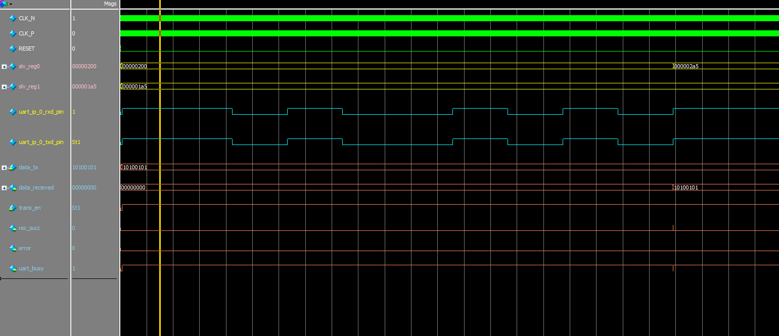
–ис 3.1 ¬ременна€ диаграмма обмена данными между процессором Microblaze и внешним цифровым устройством с использованием разработанного IP €дра UART
¬ процессе моделировани€ был рассмотрен следующий пример: процессор по шине AXI выставл€ет данные в адресуемый регистр управлени€ slv_reg1(данные дл€ передачи Ц 8 младших разр€дов регистра, сигнал начала передачи Ц 8-й разр€д регистра) дл€ передачи внешнему устройству с помощью IP €дра UART. ¬ файле тестовых воздействий выходной сигнал системы uart_ip_0_txd_pin (выход интерфейса UART) замкнут на входной uart_ip_0_rxd_pin (вход интерфейса UART).
¬ результате отрабатываетс€ передача данных по линии uart_ip_0_txd_pin и прием по линии uart_ip_0_rxd_pin с задержкой в 1 такт системной частоты. ѕрин€тые данные записываютс€ в младшие разр€ды адресуемого со стороны процессора регистра состо€ний slv_reg0, что и отображено на временной диаграмме.
4. »сходный код разработанного модул€ (описание на €зыке VerilogHDL)
1) од верхнего уровн€ модул€ интерфейса UART (файл uart_top.v)
// bit rate: 9600 kbit/sec
// clock: 100 MHz
module uart_top #(parameter FREQ = 100,
parameter RATE = 1,
|
|
|
parameter MAJ_DIV = 128)
(
input clock,
input reset_n,
input data_tx,
output data_recieved,
input trans_en,
output rec_succ,
output error,
output uart_busy,
input rxd,
output txd
);
wire clock;
wire reset_n;
wire [7:0] data_tx;
reg [7:0] data_recieved;
wire trans_en;
reg rec_succ;
reg error;
reg uart_busy;
wire rxd;
wire txd;
// LOCAL PARAMETERS
// FREQ is in MHz
// if FREQ = 100, real frequency is 100 MHz (100 000 000 Hz)
// real rate = 9600*RATE;
// if RATE = 2, real rate is 19200 bod/sec
localparam CNT_PULSES = (FREQ*1000000)/(9600*RATE);
// shift reg for TX
reg [9:0] tx_reg;
reg [13:0] tx_cnt;
reg [1:0] state_tx;
// shift reg for RX
reg [9:0] rx_reg;
reg [13:0] rx_cnt;
reg [1:0] state_rx;
reg [3:0] tx_cnt_bits;
reg [3:0] rx_cnt_bits;
reg rx_maj;
assign txd = tx_reg[0];
majority_scheme #(CNT_PULSES, MAJ_DIV)
majority_scheme_inst(
.clock(clock),
.reset_n(reset_n),
.rx_maj(rx_maj),
.rx_cnt(rx_cnt),
.maj_out_bit(maj_out_bit)
);
always @(posedge clock or negedge reset_n)
if (~reset_n)
begin
tx_reg <= 0;
rx_reg <= 0;
rx_cnt <= 0;
tx_cnt <= 0;
state_tx <= 0;
state_rx <= 0;
uart_busy <= 0;
data_recieved <= 0;
rec_succ <= 0;
rx_maj <= 0;
tx_cnt_bits <= 0;
rx_cnt_bits <= 0;
error <= 0;
end
else
begin
// One pulse
rec_succ <= 0;
// Transmitter
case (state_tx)
// idle
0: begin
if (trans_en)
state_tx <= 1;
end
// register data to transmit
1: begin
uart_busy <= 1;
tx_reg[8:1] <= data_tx;
tx_reg[9] <= 0; // stop bit
tx_reg[0] <= 1; // start bit
state_tx <= 2;
end
// transmit 10 bits
2: begin
if (tx_cnt == 10417)
begin
tx_cnt <= 0;
tx_reg[8:0] <= tx_reg[9:1];
tx_reg[9] <= 0;
tx_cnt_bits <= tx_cnt_bits + 1;
if (tx_cnt_bits == 9)
begin
state_tx <= 0;
uart_busy <= 0;
tx_cnt_bits <= 0;
end
end
else
tx_cnt <= tx_cnt + 1;
end
endcase
// Reciever
case (state_rx)
// idle
0: begin
if (rxd)
state_rx <= 1;
end
// recieve 10 bits
1: begin
rx_maj <= rxd;
if (rx_cnt_bits == 10)
begin
state_rx <= 2;
rx_cnt_bits <= 0;
end
if (rx_cnt == CNT_PULSES)
begin
rx_cnt <= 0;
rx_reg[9] <= maj_out_bit;
rx_reg[8:0] <= rx_reg[9:1];
rx_cnt_bits <= rx_cnt_bits + 1;
end
else
rx_cnt <= rx_cnt + 1;
end
// register recieved data
2: begin
data_recieved <= rx_reg[8:1];
if (~rx_reg[9])
rec_succ <= 1;
else
error <= 1;
state_rx <= 0;
end
endcase
end
endmodule
2) од мажоритарной схемы приемника модул€ UART (файл majority_scheme.v)
module majority_scheme #(parameter CNT_PULSES = 1,
parameter MAJ_DIV = 2)
(
// System
input wire clock,
input wire reset_n,
input wire [13:0] rx_cnt,
input wire rx_maj,
output reg maj_out_bit
);
localparam MIN_CNT_ONES = CNT_PULSES/(64*MAJ_DIV);
reg [2:0] cnt_ones;
always @(posedge clock or negedge reset_n)
if (~reset_n)
begin
maj_out_bit <= 0;
cnt_ones <= 0;
end
else
begin
if (rx_cnt[MAJ_DIV + 5:0] == 7'b0000000)
begin
if (rx_maj)
cnt_ones <= cnt_ones + 1;
else
cnt_ones <= cnt_ones + 0;
end
if (cnt_ones > MIN_CNT_ONES && rx_cnt == CNT_PULSES - 1)
begin
maj_out_bit <= 1;
cnt_ones <= 0;
end
else if (cnt_ones <= MIN_CNT_ONES && rx_cnt == CNT_PULSES - 1)
begin
maj_out_bit <= 0;
cnt_ones <= 0;
end
end
endmodule
3) од модул€ user_logic.v
`uselib lib=unisims_ver
`uselib lib=proc_common_v3_00_a
module user_logic
(
// -- ADD USER PORTS BELOW THIS LINE ---------------
|
|
|
// --USER ports added here
// -- ADD USER PORTS ABOVE THIS LINE ---------------
txd,
rxd,
// -- DO NOT EDIT BELOW THIS LINE ------------------
// -- Bus protocol ports, do not add to or delete
Bus2IP_Clk, // Bus to IP clock
Bus2IP_Resetn, // Bus to IP reset
Bus2IP_Data, // Bus to IP data bus
Bus2IP_BE, // Bus to IP byte enables
Bus2IP_RdCE, // Bus to IP read chip enable
Bus2IP_WrCE, // Bus to IP write chip enable
IP2Bus_Data, // IP to Bus data bus
IP2Bus_RdAck, // IP to Bus read transfer acknowledgement
IP2Bus_WrAck, // IP to Bus write transfer acknowledgement
IP2Bus_Error // IP to Bus error response
// -- DO NOT EDIT ABOVE THIS LINE ------------------
); // user_logic
// -- ADD USER PARAMETERS BELOW THIS LINE ------------
// --USER parameters added here
// -- ADD USER PARAMETERS ABOVE THIS LINE ------------
// -- DO NOT EDIT BELOW THIS LINE --------------------
// -- Bus protocol parameters, do not add to or delete
parameter C_NUM_REG = 2;
parameter C_SLV_DWIDTH = 32;
// -- DO NOT EDIT ABOVE THIS LINE --------------------
// -- ADD USER PORTS BELOW THIS LINE -----------------
// --USER ports added here
// -- ADD USER PORTS ABOVE THIS LINE -----------------
input rxd;
output txd;
// -- DO NOT EDIT BELOW THIS LINE --------------------
// -- Bus protocol ports, do not add to or delete
input Bus2IP_Clk;
input Bus2IP_Resetn;
input [C_SLV_DWIDTH-1: 0] Bus2IP_Data;
input [C_SLV_DWIDTH/8-1: 0] Bus2IP_BE;
input [C_NUM_REG-1: 0] Bus2IP_RdCE;
input [C_NUM_REG-1: 0] Bus2IP_WrCE;
output [C_SLV_DWIDTH-1: 0] IP2Bus_Data;
output IP2Bus_RdAck;
output IP2Bus_WrAck;
output IP2Bus_Error;
// -- DO NOT EDIT ABOVE THIS LINE --------------------
//----------------------------------------------------------------------------
// Implementation
//----------------------------------------------------------------------------
// --USER nets declarations added here, as needed for user logic
// Nets for user logic slave model s/w accessible register example
reg [C_SLV_DWIDTH-1: 0] slv_reg0;
reg [C_SLV_DWIDTH-1: 0] slv_reg1;
wire [1: 0] slv_reg_write_sel;
wire [1: 0] slv_reg_read_sel;
reg [C_SLV_DWIDTH-1: 0] slv_ip2bus_data;
wire slv_read_ack;
wire slv_write_ack;
integer byte_index, bit_index;
// USER logic implementation added here
// user lines
wire [7:0] data_tx;
wire trans_en;
wire [7:0] data_recieved;
wire rec_succ;
wire uart_busy;
wire error;
wire txd;
wire rxd;
assign data_tx = slv_reg1[7:0];
assign trans_en = slv_reg1[8];
uart_top uart_top_inst(
.clock(Bus2IP_Clk),
.reset_n(Bus2IP_Resetn),
.data_tx(data_tx),
.data_recieved(data_recieved),
.trans_en(trans_en),
.rec_succ(rec_succ),
.error(error),
.uart_busy(uart_busy),
.rxd(rxd),
.txd(txd)
);
// ------------------------------------------------------
// Example code to read/write user logic slave model s/w accessible registers
//
// Note:
// The example code presented here is to show you one way of reading/writing
// software accessible registers implemented in the user logic slave model.
// Each bit of the Bus2IP_WrCE/Bus2IP_RdCE signals is configured to correspond
// to one software accessible register by the top level template. For example,
// if you have four 32 bit software accessible registers in the user logic,
// you are basically operating on the following memory mapped registers:
//
// Bus2IP_WrCE/Bus2IP_RdCE Memory Mapped Register
// "1000" C_BASEADDR + 0x0
// "0100" C_BASEADDR + 0x4
|
|
|
// "0010" C_BASEADDR + 0x8
// "0001" C_BASEADDR + 0xC
//
// ------------------------------------------------------
assign
slv_reg_write_sel = Bus2IP_WrCE[1:0],
slv_reg_read_sel = Bus2IP_RdCE[1:0],
slv_write_ack = Bus2IP_WrCE[0] || Bus2IP_WrCE[1],
slv_read_ack = Bus2IP_RdCE[0] || Bus2IP_RdCE[1];
// implement slave model register(s)
always @(posedge Bus2IP_Clk)
begin
if (Bus2IP_Resetn == 1'b0)
begin
slv_reg0 <= 0;
slv_reg1 <= 0;
end
else
begin
slv_reg0[7:0] <= data_recieved;
slv_reg0[8] <= rec_succ;
slv_reg0[9] <= uart_busy;
slv_reg[10] <= error;
case (slv_reg_write_sel)
2'b10:
for (byte_index = 0; byte_index <= (C_SLV_DWIDTH/8)-1; byte_index = byte_index+1)
if (Bus2IP_BE[byte_index] == 1)
slv_reg0[(byte_index*8) +: 8] <= Bus2IP_Data[(byte_index*8) +: 8];
2'b01:
for (byte_index = 0; byte_index <= (C_SLV_DWIDTH/8)-1; byte_index = byte_index+1)
if (Bus2IP_BE[byte_index] == 1)
slv_reg1[(byte_index*8) +: 8] <= Bus2IP_Data[(byte_index*8) +: 8];
default: begin
slv_reg0 <= slv_reg0;
slv_reg1 <= slv_reg1;
end
endcase
end
end // SLAVE_REG_WRITE_PROC
// implement slave model register read mux
always @(slv_reg_read_sel or slv_reg0 or slv_reg1)
begin
case (slv_reg_read_sel)
2'b10: slv_ip2bus_data <= slv_reg0;
2'b01: slv_ip2bus_data <= slv_reg1;
default: slv_ip2bus_data <= 0;
endcase
end // SLAVE_REG_READ_PROC
// ------------------------------------------------------------
// Example code to drive IP to Bus signals
// ------------------------------------------------------------
assign IP2Bus_Data = (slv_read_ack == 1'b1)? slv_ip2bus_data: 0;
assign IP2Bus_WrAck = slv_write_ack;
assign IP2Bus_RdAck = slv_read_ack;
assign IP2Bus_Error = 0;
endmodule
ѕриложение 1. —оздание проекта в Xilinx Platform Studio

