


—одержание
» устройство дистанционного управлени€ (Infra-red remote control)ЕЕЕЕЕЕЕЕЕЕЕЕЕЕЕЕЕЕЕЕЕЕЕЕЕЕ..ЕЕЕЕЕ4
—истема управлени€ (An Evaluation System for Direct Interface of the MPX5100 Pressure Sensor with a Microprocessor)ЕЕ...............ЕЕЕЕЕ..5
Interfacing LCD Modules to the Z8 MCUЕЕЕЕЕЕЕЕЕЕЕЕЕЕЕЕЕЕЕЕЕЕЕЕЕЕЕЕ...ЕЕЕЕЕ...ЕЕЕЕЕЕЕЕЕ..6
”стройство управлени€ мощностью и напр€жением (Universal Power and Voltage Control Using the Z8E001)ЕЕЕЕЕЕЕЕЕЕЕЕЕЕ....7
Timekeeping Based on a 8-MHz Crystal (1 of 2)ЕЕЕЕЕЕЕЕЕЕЕЕЕЕЕЕЕЕЕЕЕЕЕЕЕ...ЕЕЕЕЕЕЕЕЕ..ЕЕЕЕЕЕ8
Timekeeping Based on a 60-Hz Power LineInterruptЕЕЕЕЕЕЕЕЕЕЕЕЕЕЕЕЕЕЕЕЕЕЕЕЕЕЕЕЕЕЕЕЕЕ..ЕЕЕЕЕ.9
Timekeeping Based on a 8-MHz Crystal (2 of 2)ЕЕЕЕЕЕЕЕЕЕЕЕЕЕЕЕЕЕЕЕЕЕЕЕЕЕ...ЕЕЕЕЕЕЕЕЕЕЕЕЕЕ10
÷ифровое устройство нагревани€ воды ЕЕЕЕЕЕ......ЕЕЕЕЕЕЕЕЕЕЕЕЕЕЕЕЕЕЕЕЕ...ЕЕЕЕЕЕЕЕЕЕЕЕ...Е.11
÷ифровое устройство нагревани€ воды - схема (Digital Instant Water Heater Schematic Diagram)ЕЕЕЕЕЕЕ...ЕЕЕЕ..ЕЕЕЕЕ.11
Phase ControlЕЕЕЕЕЕ...ЕЕЕЕЕЕЕЕЕЕЕЕЕЕЕЕЕЕЕЕЕЕЕЕЕЕЕЕЕЕЕЕЕЕЕЕЕЕЕЕЕЕЕЕЕ..12
Pulse Width Modulation (PWM)ЕЕЕЕЕЕ...ЕЕЕЕЕЕЕЕЕЕЕЕЕЕЕЕЕЕЕЕЕЕЕЕЕЕЕЕЕЕЕЕЕЕЕЕЕЕ12
Zero-Crossing PWMЕЕЕ...ЕЕЕЕЕЕЕЕЕЕЕЕЕЕЕЕЕЕЕЕЕЕЕЕЕЕЕЕЕЕЕЕЕЕЕЕЕЕЕЕЕЕЕЕЕ...12
Ќоль-детектор (Zero-Crossing Detection)ЕЕ...ЕЕЕЕЕЕЕЕЕЕЕЕЕЕЕЕЕЕЕЕЕЕЕЕЕЕЕЕЕЕЕЕЕЕЕЕЕ....13
“емпературный детектор (Temperature Detection)ЕЕЕЕЕЕЕЕЕЕЕЕЕЕЕЕЕЕЕЕЕЕЕЕЕЕЕЕЕЕЕЕЕЕЕЕЕ13
User InterfaceЕЕЕЕ...ЕЕЕЕЕЕЕЕЕЕЕЕЕЕЕЕЕЕЕЕЕЕЕЕЕЕЕЕЕЕЕЕЕЕЕЕЕЕЕЕЕЕЕЕЕЕЕ..14
Triac and Triac DriverЕЕЕЕЕЕЕЕЕЕЕЕЕЕЕЕЕЕЕЕЕЕЕЕЕЕЕЕЕЕЕЕЕЕЕЕЕЕЕЕЕЕЕЕЕЕЕЕЕ14
Schematic for a Dimmer Using the Z86E02 MicrocontrollerЕЕЕЕЕЕЕЕЕЕЕЕЕЕЕЕЕЕЕЕЕЕЕЕЕЕЕЕЕЕЕЕЕЕЕЕ.15
Ќедорогой аналого-цифровой преобразователь (AVR400: Low Cost A/D Converter)ЕЕЕЕЕЕЕЕЕЕЕЕЕЕЕЕЕЕЕЕЕЕЕЕ....16
8-битный прецизионный ј÷ѕ (AVR401: 8-bit Precision A/D Converter)ЕЕЕЕЕЕЕЕЕЕЕЕЕЕЕЕЕЕЕЕЕЕЕЕЕЕЕЕЕЕ.17
јналого-цифровые преобразователиЕЕЕЕЕЕ.ЕЕЕЕЕЕЕЕЕ. ЕЕЕЕЕЕЕЕЕЕЕЕЕЕЕЕЕЕЕЕЕЕЕЕЕЕЕЕ....18
Successive Approximation ADCЕЕЕЕЕЕЕЕЕЕЕЕЕЕЕЕЕЕЕЕЕЕЕЕЕЕЕЕЕЕЕЕЕЕЕЕЕЕЕЕЕЕЕЕ...18
Duty Cycle ADCЕЕЕЕЕЕЕЕЕЕЕЕЕЕЕЕЕЕЕЕЕЕЕЕЕЕЕЕЕЕЕЕЕЕЕЕЕЕЕЕЕЕЕЕЕЕЕЕЕЕ....19
Simple A/D for MCUs without built-in A/D convertersЕЕЕЕЕЕЕЕЕЕЕЕЕЕЕЕЕЕЕЕЕЕЕЕЕЕЕЕЕЕЕЕЕЕЕЕЕЕ.20
÷ифро-аналоговое преобразование (MAX529 DIGITAL-TO-ANALOG CONVERTER)ЕЕЕЕЕЕЕЕЕЕЕЕЕЕЕЕЕЕЕЕЕЕЕ...21
The R-2R DAC NetworkЕЕЕЕЕЕЕЕЕЕЕЕЕЕЕЕЕЕЕЕЕЕЕЕЕЕЕЕЕЕЕЕЕЕЕЕЕЕЕЕЕЕЕЕЕЕЕ...21
Interfacing the HC05 MCU to a Multichannel Digital-to-Analog Converter Using the C68HC705C8AЕЕЕЕЕЕЕЕЕЕЕЕЕЕЕЕЕ.22
Interfacing the HC05 MCU to a Multichannel Digital-to-Analog Converter Using the MC68HC705J1AЕЕЕЕЕЕЕЕЕЕЕЕЕЕЕЕ.23
Ўаговый двигатель (Step Motor Step Sequence)ЕЕЕЕЕЕЕЕЕЕЕЕЕЕЕЕЕЕЕЕЕЕЕЕЕЕЕЕЕЕЕЕЕЕЕЕЕЕЕЕ.24
DC MOTOR CONTROLLER USING THE ZILOG Z86E06 MCUЕЕЕЕЕЕЕЕЕЕЕЕЕЕЕЕЕЕЕЕЕЕЕЕЕЕЕЕЕЕЕЕЕ..25
DC Motor Controller SchematicЕЕЕЕЕЕЕЕЕЕЕЕЕЕЕЕЕЕЕЕЕЕЕЕЕЕЕЕЕЕЕЕЕЕЕЕЕЕЕЕЕЕЕЕЕЕЕ..26
DC Motor Controller SchematicЕЕЕЕЕЕЕЕЕЕ.ЕЕЕЕЕЕЕЕЕЕЕЕЕЕЕЕЕЕЕЕЕЕЕЕЕЕЕЕЕЕЕЕЕЕЕЕЕ.27
PID Motor Control with the Z8PE003ЕЕЕЕЕЕЕЕЕЕЕЕЕЕЕЕЕЕЕЕЕЕЕЕЕЕЕЕЕЕЕЕЕЕЕЕЕЕЕЕЕЕЕЕ....28
Limit SensorsЕЕЕЕЕЕЕЕЕЕЕЕЕЕЕЕЕЕЕЕЕЕЕЕЕЕЕЕЕЕЕЕЕЕЕЕЕЕЕЕЕЕЕЕЕЕЕЕЕЕЕЕ.29
|
|
|
H-BridgeЕЕЕЕЕЕЕЕЕЕЕЕЕЕЕЕЕЕЕЕЕЕЕЕЕЕЕЕЕЕЕЕЕЕЕЕЕЕЕЕЕЕЕЕЕЕЕЕЕЕЕЕЕЕ.29
AVR242: 8-bit Microcontroller Multiplexing LED Drive and a 4 x 4 KeypadЕЕЕЕЕЕЕЕЕЕЕЕЕЕЕЕЕЕЕЕЕЕЕЕЕЕЕЕЕ..30
Circuit Diagram for Keypad/Display UnitЕЕЕЕЕЕЕЕЕЕЕЕЕЕЕЕЕЕЕЕЕЕЕЕЕЕЕЕЕЕЕЕЕЕЕЕЕЕЕЕЕ.30
Theory of Operation ЕЕЕЕЕЕЕЕЕЕЕЕЕЕЕЕЕЕЕЕЕЕЕЕЕЕЕЕЕЕЕЕЕЕЕЕЕЕЕЕЕЕЕЕЕЕЕЕЕ..31
Keypad and LED connections (AVR240: 4 x 4 Keypad Ц Wake up on Keypress)ЕЕЕЕЕЕЕЕЕЕЕЕЕЕЕЕЕЕЕЕЕЕЕЕЕЕЕЕ32
» приемник дистанционного управлени€ (AVR410: RC5 IR Remote Control Receiver)ЕЕЕЕЕЕЕЕЕЕЕЕЕЕЕЕЕЕЕЕЕЕЕ..33
—хема формировани€ DTMF сигнала (DTMF Tone Generation Using the Z86E04 MCU)ЕЕЕЕЕЕЕЕЕЕЕЕЕЕЕЕЕЕЕЕЕЕЕ...34
—хема формировани€ DTMF сигнала (DTMF Tone Generation Using the Z86E04 MCU)ЕЕЕЕЕЕЕЕЕЕЕЕЕЕЕЕЕЕЕЕЕЕЕ...35
—хема телефонной трубки DTMF сигнала (Telephone Handset with DTMF using the 68HC05F4)ЕЕЕЕЕЕЕЕЕЕЕЕЕЕЕЕЕЕЕ.....36
—хема ЕЕЕЕЕЕЕЕЕЕЕЕЕЕЕЕЕЕЕЕЕЕЕЕЕЕЕЕЕЕЕЕЕЕЕЕЕЕЕЕЕЕЕЕЕЕЕЕЕЕЕЕЕЕЕЕЕ.37
—хема управлени€ фазой (Power Phase Control Using Z8 Microcontrollers)ЕЕЕЕЕЕЕЕЕЕЕЕЕЕЕЕЕЕЕЕЕЕЕЕЕЕЕЕЕ.38
анал широтно-импульсной модул€ции (1 Channel DAC Using A PWM)ЕЕЕЕЕЕЕЕЕЕЕЕЕЕЕЕЕЕЕЕЕЕЕЕЕЕЕЕЕ.40
—хема мультиплексировани€ (Multiplexing Four 7-segments LEDs)ЕЕЕЕЕЕЕЕЕЕЕЕЕЕЕЕЕЕЕЕЕЕЕЕЕЕЕ.ЕЕЕЕ....41
—хема мультиплексировани€ с клавиатурой 4 на 4 (Multiplexing Four 7-segments LEDs with a 4 x 4 Keypad)ЕЕЕЕЕЕЕЕЕЕЕЕЕЕ...42
4х канальный вольтметр с клавиатурой и дисплеем (Four Channel Voltmeter with Display And Keypad)ЕЕЕЕЕЕЕЕЕЕЕЕЕЕЕЕЕ43
SRAM Block Schematic (STK 501)ЕЕЕЕЕЕЕЕЕЕЕЕЕЕЕЕЕЕЕЕЕЕЕЕЕЕЕЕЕЕЕЕЕЕЕЕЕЕЕЕЕЕЕЕ.Е..44
—хемаЕЕЕЕЕЕЕЕЕЕЕЕЕЕЕЕЕЕЕЕЕЕЕЕЕЕЕЕЕЕЕЕЕЕЕЕЕЕЕЕЕЕЕЕЕЕЕЕЕЕЕЕЕЕЕЕЕ..45
—хема звукового термометра (Audible Thermometer Schematics)ЕЕЕЕЕЕЕЕЕЕЕЕЕЕЕЕЕЕЕЕЕЕЕ.ЕЕЕЕЕЕЕЕЕЕ46
јвтоматический регул€тор напр€жени€ЕЕЕЕЕЕЕЕЕЕЕЕЕЕЕЕЕЕЕЕЕЕЕЕЕЕЕЕЕЕЕЕЕЕЕЕЕЕЕЕЕЕЕ.47
—хема автоматического регул€тора напр€жени€ЕЕЕЕЕЕЕЕЕЕЕЕЕЕЕЕЕ.ЕЕЕЕЕЕЕЕЕЕЕЕЕЕЕЕЕЕЕЕ.47
Voltage Regulator InputЕЕЕЕЕЕЕЕЕЕЕЕЕЕЕЕЕЕЕЕЕЕЕЕЕЕЕЕЕЕЕЕЕЕЕЕЕЕЕЕЕЕЕЕЕЕЕЕ.48
Voltage Regulator OutputЕЕЕЕЕЕЕЕЕЕЕЕЕЕЕЕЕЕЕЕЕЕЕЕЕЕЕЕЕЕЕЕЕЕЕЕЕЕЕЕЕЕЕЕЕЕЕ..48
Interfacing the MC68HC705J1A to 9356/9366 EEPROMsЕЕЕЕЕЕЕЕЕЕЕЕЕЕЕЕЕЕЕЕЕЕЕЕЕЕЕЕЕЕЕЕЕЕЕЕЕ49
Evaluation Board: MemoriesЕЕЕЕЕЕЕЕЕЕЕЕЕЕЕЕЕЕЕЕЕЕЕЕЕЕЕЕЕЕЕЕЕЕЕЕЕЕЕЕЕЕЕЕЕЕЕЕ...50
Evaluation Board: Power, Crystal Oscillator, Clock Distribution and Power Supply ShutdownЕЕЕЕЕЕЕЕЕЕЕЕЕЕЕЕЕЕЕЕЕЕ...51
Evaluation Board: Push Buttons, LEDs, Reset and Serial InterfaceЕЕЕЕЕЕЕЕЕЕЕЕЕЕЕЕЕЕЕЕЕЕЕЕЕЕЕЕЕЕЕЕЕ...52
÷ифровой диктофон (Digital Sound Recorder with AVR and DataFlash: Microcontroller and Memory Circuit Diagram)ЕЕЕЕЕЕЕЕЕЕЕ...53
÷ифровой диктофон (Digital Sound Recorder with AVR and DataFlash: Microphone and Speaker Circuit Diagram)ЕЕЕЕЕЕЕЕЕЕЕЕЕ.54
ћакетно-отладочна€ плата. ѕринципиальна€ схемаЕЕЕЕЕЕЕЕЕЕЕЕЕЕЕЕЕЕЕЕЕЕЕЕЕЕЕЕЕЕЕЕЕЕЕЕЕ.....55
ћакетно-отладочна€ плата. ѕринципиальна€ схема (продолжение)ЕЕЕЕЕЕЕЕЕЕЕЕЕЕЕЕЕЕЕЕЕЕЕЕЕЕЕЕЕЕЕ...56
онтроллер-конструкторЕЕЕЕЕЕЕЕЕЕЕЕЕЕЕЕЕЕЕЕЕЕЕЕЕЕЕЕЕЕЕЕЕЕЕЕЕЕЕЕЕЕЕЕЕЕЕЕЕ..57
”правление LCD дисплеем (DIRECT DRIVE OF LCD DISPLAYS)ЕЕЕЕЕЕЕЕЕЕЕЕЕЕЕЕЕЕЕЕЕЕЕЕЕЕЕЕЕЕЕ....58
÷епь управлени€ (LCD Direct Drive Demo Circuit)ЕЕЕЕЕЕЕЕЕЕЕЕЕЕЕЕЕЕЕЕЕЕЕЕЕЕЕЕЕЕЕЕЕЕЕЕ...58
Multiple BackplanesЕЕЕЕЕЕЕЕЕЕЕЕЕЕЕЕЕЕЕЕЕЕЕЕЕЕЕЕЕЕЕЕЕЕЕЕЕЕЕЕЕЕЕЕЕЕЕЕЕ..59
PIC17C4X EXTERNAL RAM SCHEMATICЕЕЕЕЕЕЕЕЕЕЕЕЕЕЕЕЕЕЕЕЕЕЕЕЕЕЕЕЕЕЕЕЕЕЕЕЕЕЕЕЕ...60
|
|
|
лавиатура (HC05 MCU Keypad Decoding Techniques Using the MC68HC705J1A)ЕЕЕЕЕЕЕЕЕЕЕЕЕЕЕЕЕЕЕЕЕЕЕЕЕ...61
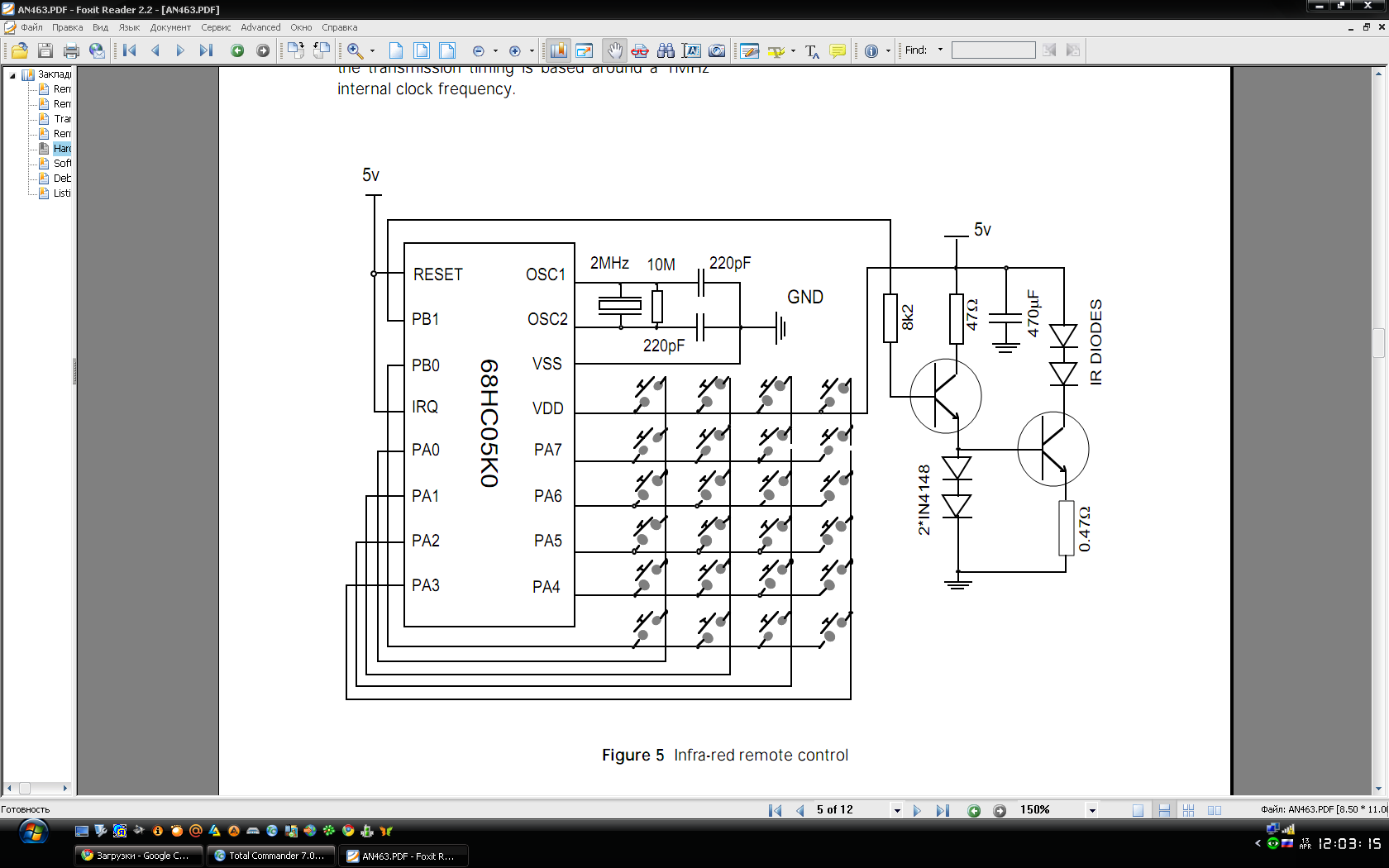
–исунок 1 Ц » устройство дистанционного управлени€ (Infra-red remote control)
After the initial set-up of the ports as inputs or outputs the remote control goes into STOP mode. It will remain in STOP mode as long as the device is not reset or a key is not pressed. When a key is pressed an interrupt request is generated. A short time delay makes sure that it is a true key press and not noise and also allows time for any switching effects on the inputs to pass prior to checking the inputs.
The keyboard is then read to find which key has been pressed and the code for the key is decoded into an instruction and transmitted to the television. If the key is held down the instruction is re-transmitted until the key is released. This is useful for the instructions which count through the television channels or adjust the volume, color or brightness controls. When the key is released a terminating instruction is sent to the receiver to inform it that the next message received is a separate instruction. This is useful in the case of a one time instruction like sending a channel number. In this example the receiver will tune to a channel only once; to tune to another channel the key must be released and a new instruction sequence received. After terminating the transmission the ports are reset ready for the next key press and the processor returns to the STOP mode.

–исунок 2 Ц —истема управлени€ (DEVB-114 System Schematic: An Evaluation System for Direct Interface of the MPX5100 Pressure Sensor with a Microprocessor)

–исунок 3 Ц Interfacing LCD Modules to the Z8 MCU

–исунок 4 Ц ”стройство управлени€ мощностью и напр€жением
(Universal Power and Voltage Control Using the Z8E001)

–исунок 5 Ц Timekeeping Based on a 8-MHz Crystal (1 of 2)
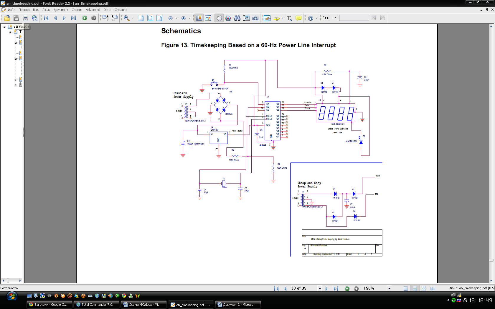
–исунок 6 Ц Timekeeping Based on a 60-Hz Power Line Interrupt
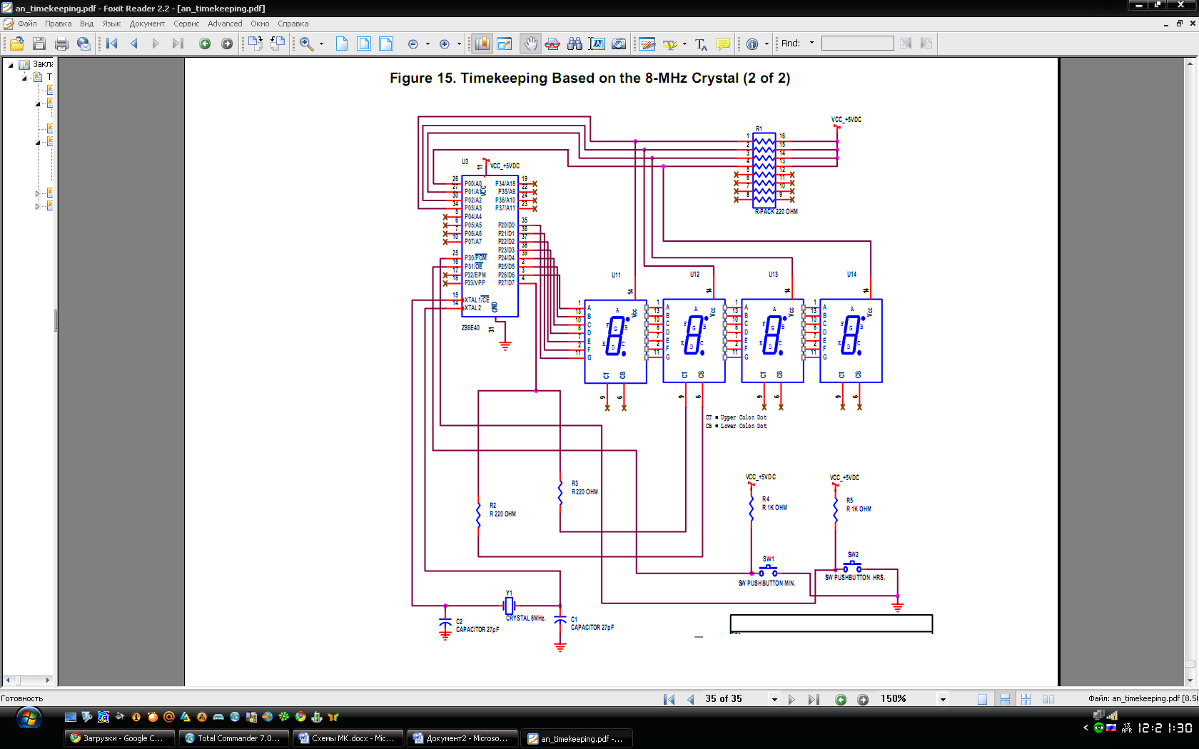
–исунок 7 Ц Timekeeping Based on a 8-MHz Crystal (2 of 2)
 Digital Instant Water Heater Schematic Diagram
–исунок 8 Ц ÷ифровое устройство мгновенного нагревани€ воды
(Digital Instant Water Heater Schematic Diagram)
THEORY OF OPERATION
The conventional method of control is plain and simple: On/OffЧfull power or no power, and nothing in between. With the Z8ЃMCU, the power duty cycle can be controlled in a number of ways that vary the percentage of heater power output. The three common duty cycle control methodsЧPhase Control, Pulse-Width Modulation (PWM), and Zero-Crossing PWMЧwill each be discussed.
Phase Control
 The phase control method conducts power during a specific time period in each half of the 50/60 Hz AC power cycle. Triacs are commonly used to switch on/off the
power to loads in AC power systems applications. A gate voltage is required to turn on a triac. Once УOn,Ф the triac will generate substantial current to maintain its gate voltage until the AC sine wave approaches zero voltage. The water power duty cycle can be controlled by simply controlling the fire angle (turn on start time). The triac will deliver the power to load after the fire angle and turn off at the zero-crossing point.
Phase control can be easily implemented with a triac and a few passive components. However, the relationship between the firing angle and the power ratio is not linear. Getting an exact proportional output power is somewhat difficult. In addition, switching the triac on at the firing angle may induce high EMI. For a 220V AC line, switching at the peak voltage (311V) will generate a very high EMI noise, as an example. The European Community has imposed some restrictions on the EMI generation of an electrical appliance. Such EMI noise must be suppressed or reduced if the appliance is exported to Europe. As a complementary solution, a snubber or an EMI filter may be added to reduce the noise.
|
|
|
Pulse Width Modulation (PWM)
 There are always highs and lows in cyclical signals. By controlling the width of the highs (Ta) and lows (Tb), the percentage of power (up to full power) delivered to the load can be controlled. PWM is a technique by which the power ratio is controlled by varying the duty cycle of signal high time to total cycle time of the
cyclical signal. In this application, the cyclical signal is the AC power line.
One of the advantages of using PWM is its ease of implementation and subsequent lower cost; however, there are trade-offs to consider. Since the AC waveform is not linear, the power delivered during the peak voltage time will be higher than during the zero-crossing time, which means that power delivery is not linear. Also, the
frequency of the PWM signal will affect the smoothness of the power delivered. Generally, higher PWM frequency results in better smoothness. Finally, the On/Off switching of the PWM signal will induce EMI noise, which the designer must
minimize.
Zero-Crossing PWM
 Since our application uses the AC line at 50/60 Hz, this is the PWM frequency of any PWM power control methodology. Because the power delivery will be relatively unsmooth, the previously discussed PWM technique can be combined with a zero-crossing switching technique to form a Уzero-crossing PWMФ technique. With AC lines at 50/60 Hz, the zero-crossing PWM technique combines the ease of implementing the PWM methodology while minimizing the EMI noise induced and smoothing the power delivery, which are some of the benefits of the zero-crossing switching technique.
The AC power line is a sine wave with its peak voltage at π / 2 and minimum at 0 or π. If the power line frequency is 60 Hz, there will be 120 (60 Hz x 2) crossings. Power is turned on and off only at the zero-crossing point. Thus, the EMI will be minimized, and the power applied is smoothed as much as possible.
For example, if delivery of 25 percent of full power is desired, one AC cycle for every four AC cycles of appliance power will be turned on. This means that there are three УOffФ AC cycles for every four AC cycles. Since the power potential of each cycle should be the same, there is a 25 percent power ratio. This method is also called УCycle Skipping.Ф
Ќоль-детектор (Zero-Crossing Detection)
 A Z8ЃMCU controls the power level and senses the water temperature through a thermistor. The Z8 MCU detects the zero-crossing points of the AC power line and applies or removes AC power to the heating elements of the water heater as needed. Refer to Figure 5 for the zero-crossing detection circuitry.
The AC power line is reduced by the potential divider resistors, R1 and R2. Since R2 is 1/100th of R1, the line voltage is divided by 100 times.
VIN = AC Line Voltage x R2 / (R1 + R2)
where VIN > -0.7V
Diode D1 is used to clamp the negative input voltage VIN to -0.7V minimum. Too much negative voltage may damage the MCU. The half AC waveform is connected to the positive input of the Z8 comparator (P31). Prior to zero-crossing detect, port pin P35 of the Z8 is cleared Low so that the reference input of the comparator
at P33 is zero volt. When the half AC waveform moving from positive to negative, the comparator output changes from one to zero. The edges of the comparator output signal corresponds to the zero-crossing points of the AC power line. By monitoring this signal, the zero-crossing point can be detected.
International Power Line Considerations Power line voltages vary from country to country and may be particularly unstable in some developing countries. For
|
|
|
example, a peak voltage may drop by as much as 10V when a 15A load is connected. In this case, the zero-crossing switch must be 10 Hz (or higher). The switching frequency can be doubled by switching at every half-cycle. (The power line has two zero crossings at an angle equal to 0 or π.)
“емпературный детектор (Temperature Detection)

The resistance of a thermistor changes with temperature.
If current is applied through a thermistor and voltage across it measured against a reference voltage, the temperature can be approximated. The comparators in a Z8Ѓ MCU provide an economical way of measuring water temperature with a thermistor.
Figure 6 shows a simple scheme by which the thermistor voltage (VCC-VT) can be determined as a function of the thermistor resistance RT and the 6.8K ohm resistor, which is shown.
User Interface
 There are eight levels of selected water temperature. The power-up default is at the preset level 4. The user can select warmer and cooler by pressing the UP and DOWN buttons, respectively. The LEDs indicate the selected level.
The R4 and R6 10K ohm resistors are used to reduce the Electrostatic Discharge (ESD) current to the Z8Ѓ MCU. These two resistors are removable if ESD is not an issue for the product.
Triac and Triac Driver
 A triac is commonly used for duty-cycle control. Similar to a relay, a triac can be On and Off with a relatively small amount of current. Unlike a relay, its response time is much faster and will not generate electric sparks at the moving contact point. An initial current of approximately 50 mA for 40 µS is needed to start it. (Different triacs have different characteristics, so the 50 mA current and 40 µS time are for reference only.) After the triac is On, a self generated current is essential to maintain the On status. The triac will turn Off automatically when the line voltage is dropped to zero as the self-generated current will also be zero when line voltage is zero.
A triac driver is used to provide a high current to drive the triac. An opto-driver is used if primary and secondary isolation is required. When the Z8 MCU P36 outputs a zero, the internal LED is On, and the triac driver will turn on the triac. With the AC passing the loading (heater coil), the water is heated up to the desired temperature.
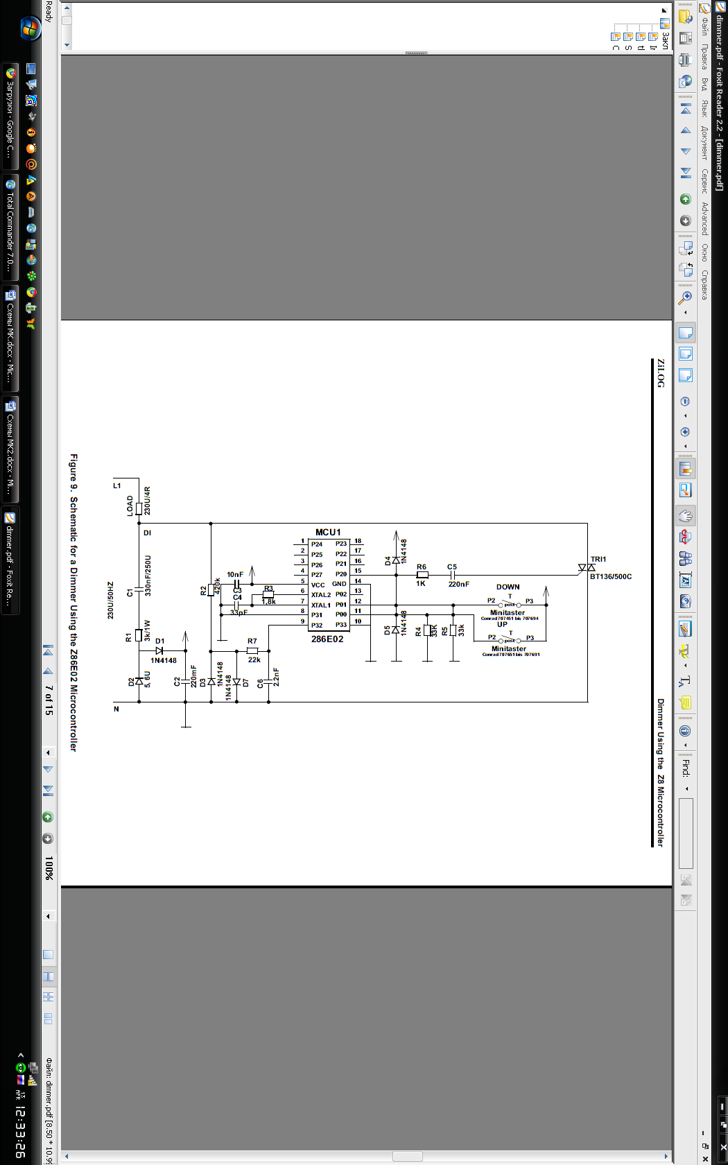
–исунок 9 Ц Schematic for a Dimmer Using the Z86E02 Microcontroller

–исунок 10 Ц Ќедорогой аналого-цифровой преобразователь (AVR400: Low Cost A/D Converter)
This application note targets cost and space critical applications that need an ADC. It describes how to make a simple ADC with only two external components, a resistor and a capacitor. The design enables a very compact and inexpensive application.
Theory of Operation
Nearly all AVR microcontrollers feature an analog comparator which makes it easy to implement an ADC. The signal to b e m e a s u r e d i s c o n n e c t e d t o t h e inverted input, and a reference signal is connected to the non-inverting input. The reference signal is generated by charging a capacitor through a resistor. When the capacitor is being charged, the voltage across it will follow an exponential curve. If the voltage range to be measured is limited to 2/5*VC C, the exponential curve is a good approximation to a straight line. The voltage of the applied signal, UIN is found by measuring the time it takes for the voltage across the capacitor to rise above the applied voltage. By using one pin on port B to control the charging and discharging of the capacitor, only three port pins are used.
 This application note describes how to perform a kind of dual slope A/D conversion with an AVR microcontroller. The converter is very low cost, requiring only six discrete components in addition to the AVR. Five of the controller pins are used. This example is based on the AT90S1200 device, but any AVR device with a comparator can be used.
Theory of Operation
The capacitor is charged with a constant current supplied by the transistor. The capacitor voltage will rise linearly. To discharge the capacitor, the AIN0-pin is set
to output with a С0Т applied. A reference voltage at VCC/2 is supplied by the resistor network Rref1 and Rref2. When the PB1 and PB2-pins are configured as
inputs, the reference is turned off, and the voltage level at the AIN1-pin will be the input voltage Vin. By setting the pins as outputs and applying a С0Т and a С1Т,
the level at the AIN1-pin will be VCC/2 (if the resistors are of equal size). The input resistor Rin have to be at least 100 times higher than the reference resistors Rref1
|
|
|
and Rref2 to avoid measurement errors.
The algorithm used for the conversion is as follows:
1. Turn on the reference
2. Charge the capacitor until the reference voltage is
reached. Measure the time needed for this, Tref
3. Turn off the reference and discharge the capacitor
4. Charge the capacitor until the input voltage is
reached. Measure the time needed for this, Tin
–исунок 11 Ц 8-битный прецизионный ј÷ѕ (AVR401: 8-bit Precision A/D Converter)
јналого-цифровые преобразователи:

Successive Approximation ADC
For applications requiring fast conversion times, consider the successive approximation method. This method uses a Digital-to-Analog Converter (DAC) in its feedback loop. The DAC is comprised of an R2R ladder connected to port P2. When a binary value is output at Port 2, a DC voltage proportional to the binary value appears at pin 1 of the ladder network. The DAC completes a binary search on the input voltage. This search is achieved by first setting the most significant bit (MSB) of the DAC and testing the comparator output. If the comparator output is 0, the DAC output for this bit is set to 0. If the comparator output is 1, then the DAC output for this bit is set to 1. The bits from output port 2 are individually tested in ascending order, performing the same test. When all the bits are tested, the conversion is complete. The output from the R2R resistor network becomes the comparator's reference voltage. The analog voltage to be measured can be connected to either P31 or P32, the non-inverting inputs of the comparators.
To start the conversion, the MSB of P2 is set, resulting in a voltage of.5 Vcc at the VREF input of the comparator. If Vcc is 5V, then the voltage is 2.5V. The non inverting comparator input is tested. If High, then the analog voltage must be 2.5V–5.0V.
The next bit, P26, is set, and the input port is tested again. If LOW, then bit P26 is reset. The process continues until all bits of P2 are tested. The resultant value at
P2 is the digital representation of the analog input. With a crystal frequency of 8 MHz, the conversion time is approximately 110 µS. Even more resolution is avail-
able from 10- and 12-bit R2R networks. Of course, more resolution requires more port pins.
–исунок 12 Ц ј÷ѕ последовательного приближени€

Duty Cycle ADC
When speed is not important, a Duty Cycle Analog to Digital Converter is the perfect solution. This method works by measuring the time it takes a capacitor to
charge up above the input voltage and discharge below the input voltage.
Because the charge time is compared to the discharge time, component tolerances have no effect on accuracy, and the reading is linear. In addition to the comparators, only one port pin is required to control the RC network, leaving the balance of the I/O free. This example performs a two-channel, 11 bit conversion.
Because this method is based upon measuring time, the duty cycle ADC requires a stable time base. The stable time base is accomplished using only one interrupt
for the timer and ensuring that the software’s charge and discharge paths execute in the same amount of time.1
At each timer interrupt period, the capacitor is compared to the input voltage. If the capacitor is greater than the input voltage, than the capacitor is discharged
and the pass counter is decremented. If the capacitor is less than the input voltage, the capacitor is charged, the reading is incremented, and the pass counter is
decremented. When the pass counter reaches 0 the conversion is complete. For highest stability, the capacitor must be charged to the input voltage before
measurement begins. The easiest way to charge the capacitor to the input voltage is to perform two conversions and discard the first one. Also, the total conversion
time must be an even multiple of the line frequency (60Hz or 50Hz). This example is 2048 counts x 130 µ S = 266mS, approximately 16 cycles at 60 Hz, with
a 1M resistor and a.1 µ F capacitor. Total conversion time for both channels is 1.06S.
–исунок 13 Ц ј÷ѕ циклического преобразовани€
Simple A/D for MCUs without built-in A/D converters:

Block diagram:
ЦThere are four I/Os used on the MCU.
ЦADCTL is used both as an output and as an input.
ЦADINP is always a high impedance input.
ЦTwo outputs are used for debugging the system.
ЦSCITR is used to transmit the result serially.
ЦSYNC is a triggered signal for an external oscilloscope.
The conversion is divided into a calibration phase and a measurement phase.
Calibration phase
The calibration phase finds the R1*C time constant. This is done by first discharging the external capacitor C by pulling ADCTL low. Notice that the resistors Rx + R2 have no effect at all at this time.
 Measurement phase
Then ADCTL is pulled high towards Vdd to charge the capacitor C. The time, Tc depending on R1*C, is measured to reach the threshold voltage, Vref, of ADINP. When the input signal passes the threshold level, the elapsed time is measured and stored. In other words the calibration time is:
Tc = R1 * C * ln(Vdd/(Vdd - Vref))
After the measurement, ADCTL is pulled low to discharge the capacitor C again.
The second measurement step makes the ADCTL go high impedance. The capacitor C immediately starts to charge. The time taken is given by the formula:
Tm = (R1 + R2 + Rx) * C * ln(Vdd/(Vdd - Vref))
The time to reach the threshold voltage is measured again. To make things simple we shall set R1 and R2 each equal to R.
Tm = (R + R + Rx) * C * ln(Vref/(Vref - Vr)
The final result is calculated to get correct scaling.
Tf = Tm - 2 * Tc
Substitute with the values calculated before and replace the ln(Vref/(Vref - Vr) with K.
Tf = ((2 * R + Rx) - 2 * R) * K
Tf = Rx * K
Which gives the final result Rx = Tf/K
÷ифро-аналоговое преобразование (MAX529 DIGITAL-TO-ANALOG CONVERTER)
The MAX529 is a monolithic device consisting of eight voltage output DACs. Two reference voltage inputs feed two sets of four DACs on the chip. A serial interface is used to communicate with the chip. The MAX528 operates from split supplies totaling up to 20 V, including +5 V and -15 V, +12 V and -5 V, and +15 V and -5 V, or a single supply up to 15 V. The MAX529 operates from -5 V supplies or from a single +5 V supply. This application note utilizes the MAX529 with a single +5 V supply. If low-power consumption is required, the part can be put in shutdown mode with its shutdown pin. During shutdown, the part uses less than 50 нA of current. The part can configure its buffer mode of the DAC output pins in three different ways:
1) An unbuffered mode connects the internal R-2R DAC network directly to the output pin.
2) A full-buffered mode inserts an op amp buffer between the R-2R network and the output pin, providing a +5 mA and -2 mA output drive.
3) A half-buffered mode is similar to the full-buffered mode but only provides up to +5 mA of output drive in a unipolar configuration.
If needed, the part can be serially daisy-chained to other 529s to increase the number of DACs in a system.
The R-2R DAC Network
The DAC inside the MAX529 is based on the R-2R resistor network. Most CMOS DACs are based on the R-2R current steering circuit. Figure 1 shows a simple 2-bit R-2R DAC. A reference voltage is applied to the VREF pin and the current, I, is binary divided throughout the array as shown. These currents are steered in discrete incremental amounts to the OUT1 and OUT2 nodes. The digital input to the DAC determines the position of the switches used to steer the current. A logic one causes the switch to steer the current to OUT1, while a logic zero causes the switch to steer the current to OUT2. OUT2 is at analog ground. The feedback configuration of the op amp forces OUT1 to be at virtual ground potential.

–исунок 14 Ц Simple 2-Bit Digital-to-Analog Converter

–исунок 15 Ц Interfacing the HC05 MCU to a Multichannel Digital-to-Analog Converter Using the C68HC705C8A
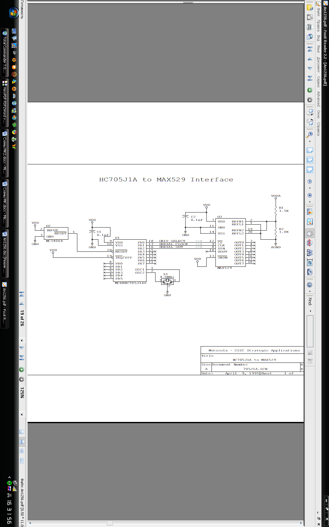
–исунок 16 Ц Interfacing the HC05 MCU to a Multichannel Digital-to-Analog Converter Using the MC68HC705J1A
Ўаговый двигатель (Step Motor Step Sequence)
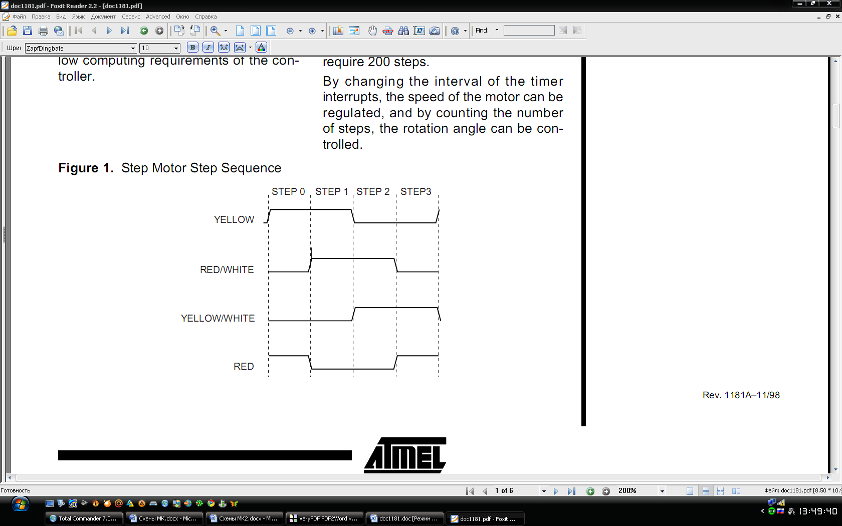
This application note describes how to implement a compact size and high speed interrupt driven step motor controller. Step motors are typically used in applications like camera zoom/film feeder, fax machines, printers, copying machines, paper feeders/sorters and disk drives. The high performance of the AVR controller enables the designer to implement high speed step motor applications with low computing requirements of the controller.
Theory of Operation
A DC step motor translates current pulses into motor rotation. A typical motor contains four winding coils. The coils are often labeled red, yellow/white, red/white and yellow, but may have other colors. Applying voltage to these coils forces the motor to step one step. In normal operation, two winding coils are activated at the same time. The step motor moves clockwise one step per change in winding activated. If the sequence is applied in reverse order, the motor will run counterclockwise. The speed of rotation is controlled by the frequency of the pulses. Every time a pulse is applied to the step motor the motor will rotate a fixed distance. A typical step rotation is 1.8 degrees. With 1.8 degree rotation in each step will a complete rotation of the motor (360 degrees) require 200 steps. By changing the interval of the timer interrupts, the speed of the motor can be regulated, and by counting the number of steps, the rotation angle can be controlled.
Table shows the hexadecimal values to be output to the step motor to perform each step:
 –исунок 17 Ц ¬ременна€ диаграмма работы
DC MOTOR CONTROLLER USING THE ZILOG Z86E06 MCU Ц рисунок 18:
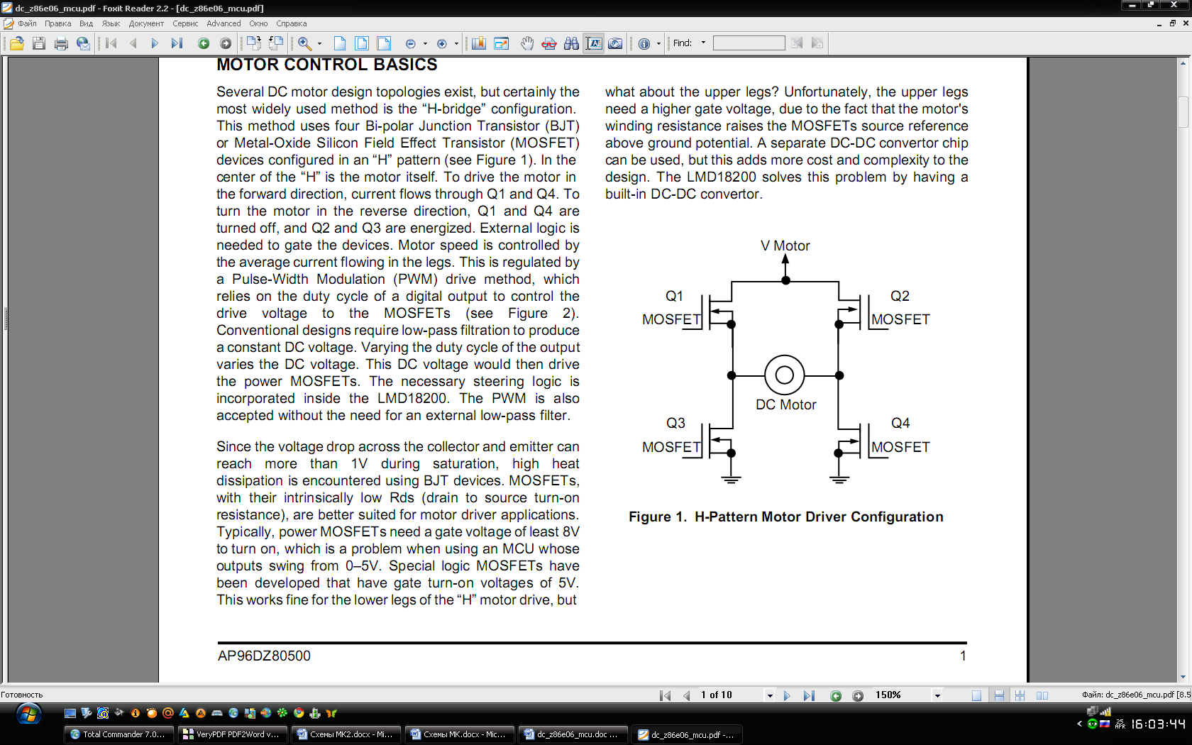
Several DC motor design topologies exist, but certainly the most widely used method is the УH-bridgeФ configuration. This method uses four Bi-polar Junction Transistor (BJT) or Metal-Oxide Silicon Field Effect Transistor (MOSFET) devices configured in an УHФ pattern. In the center of the УHФ is the motor itself. To drive the motor in the forward direction, current flows through Q1 and Q4. To turn the motor in the reverse direction, Q1 and Q4 are turned off, and Q2 and Q3 are energized. External logic is needed to gate the devices. Motor speed is controlled by the average current flowing in the legs. This is regulated by a Pulse-Width Modulation (PWM) drive method, which relies on the duty cycle of a digital output to control the drive voltage to the MOSFETs. Conventional designs require low-pass filtration to produce a constant DC voltage. Varying the duty cycle of the output varies the DC voltage. This DC voltage would then drive the power MOSFETs. The necessary steering logic is incorporated inside the LMD18200. The PWM is also accepted without the need for an external low-pass filter.
Since the voltage drop across the collector and emitter can reach more than 1V during saturation, high heat dissipation is encountered using BJT devices. MOSFETs, with their intrinsically low Rds (drain to source turn-on resistance), are better suited for motor driver applications. Typically, power MOSFETs need a gate voltage of least 8V to turn on, which is a problem when using an MCU whose outputs swing from 0Ц5V. Special logic MOSFETs have been developed that have gate turn-on voltages of 5V.
This works fine for the lower legs of the УHФ motor drive, but what about the upper legs? Unfortunately, the upper legs need a higher gate voltage, due to the fact that the motor's winding resistance raises the MOSFETs source reference above ground potential. A separate DC-DC convertor chip can be used, but this adds more cost and complexity to the design. The LMD18200 solves this problem by having a built-in DC-DC convertor.
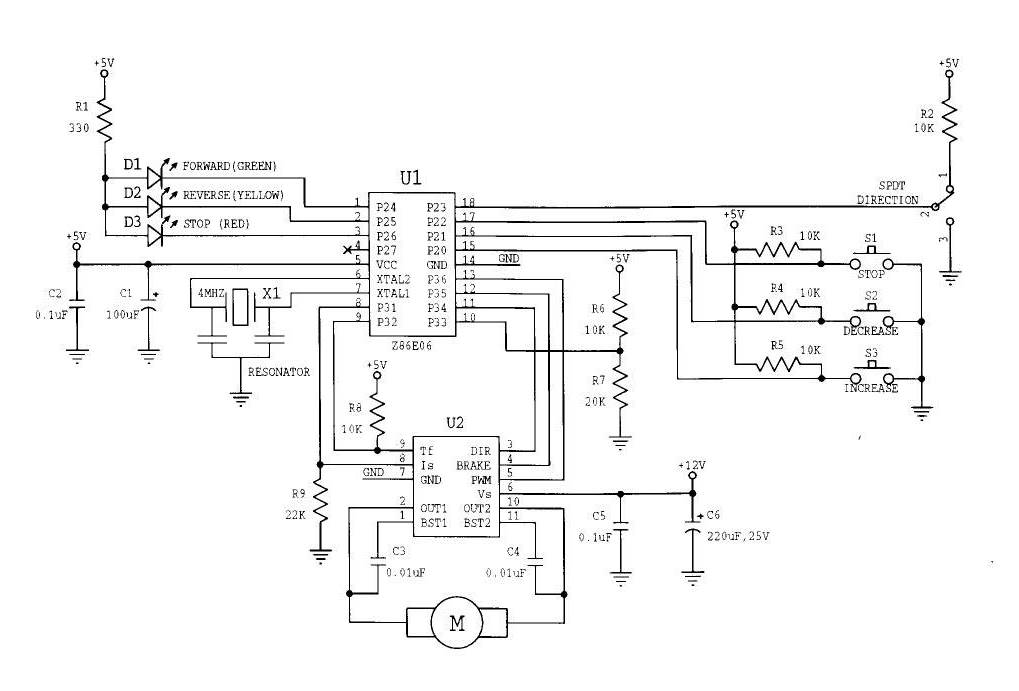
–исунок 19 - DC Motor Controller Schematic
–исунок 20 - DC Motor Controller Schematic

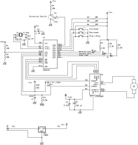
–исунок 21 - PID Motor Control with the Z8PE003
Limit Sensors

The limit sensors consist of a slotted detector with an optical IR light-emitting diode (LED) and a phototransistor in a plastic housing. The signal is broken when an object is passed through the gap in the housing. Breaking this transmit signal turns off the base current to the phototransistor, turning off the phototransistor. The output signal is then pulled to a logic High level on the Z8PE003.
 The LED turns on the phototransistor when there is no object in the optical path, pulling the output signal to a Low. A resistor in series with the LED limits the current to 18 mA. LEDs DLIM1 and DLIM2 illustrate when the phototransistor is turned on.
H-Bridge
The H-Bridge regulates motor speed by controlling the average current applied to the motor. The pulse-width modulated signal from the Z8PE003 controls the amount of time each leg of the H-Bridge is on or off. The longer the on time, the more average current is applied, and the faster the motor spins. The LMD18200 features special logic inputs that are TTL- and CMOS-compatible to turn on the MOSFETs. The voltage developed across R11 sets the current limit flag. The following equation determines the R11 value. Note that the value used in the calculation is the load current for this application, not the stall current, because of the near no-load condition on the motor.
R = 5 Volts ÷ (377 µA ÷ A x 275 mA) = 48KΩ
The function of the thermal overload flag is to warn the Z8PE003 when the temperature inside the H-Bridge reaches the 145∞C warning limit. Should this limit be reached, the Z8PE003 can shut down the system before the H-Bridge reaches the shut-down temperature of 170∞C. The motor is a generic, permanent magnet DC motor with a 100:1 ratio output gear train. It operates in a 4.5 to 12 VDC operating range, 75-mA no-load current, and 69 rpm no-load speed.

