The junction breakdown characteristics due to impact ionization and tunneling should be already in good agreement with measurements at room temperature. Nevertheless, in some cases, a fine-tuning of model parameters may be necessary. The onset of breakdown is influenced mainly by the doping profile (gradient), the bending of material interfaces (for example, LOCOS bird’s beak), and the doping profile corner effects (3D).
The temperature dependence of impact ionization must be calibrated as well to obtain the correct behavior at high temperatures. Ideally, breakdown voltage measurements at different temperatures are used for this purpose.
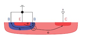
For calibrating the snapback point (It1, Vt1), the most important quantity is the effective base resistance Rb of the bipolar device (or the inherent parasitic bipolar device between the drain, body, and source in the case of MOS). Bipolar snapback is triggered after the collector-base junction is driven into avalanche breakdown (see Figure 5).

«Fig. 5.». Schematic cross section of NPN transistor (or parasitic NPN transistor in MOS case) showing carrier flow in snapback operation.
As a result, in the case of NPN, the impact-generated hole current is conducted from the avalanche region (G) through the p-region to the base contacts. Consequently, the hole current causes a voltage drop across the Rb, which induces a forward bias to the base‑emitter junction. Eventually, a sufficient base-emitter current flow results in the triggering of the NPN transistor. The positive feedback loop formed by increasing impact ionization and increasing forward bias of the base-emitter junction produces the well-known voltage snapback behavior with a negative differential resistance (NDR) regime until a holding voltage Vh is reached.
The calibration of the snapback current level It1 may require some adjustment of the parameters of the low-field mobility model for low- and medium-range temperatures because self-heating may play a role. If evidence of inhomogeneous current flow is found (inhomogeneous triggering [6]), it is necessary to use 3D simulations to correctly predict snapback behavior (see Example of 3D ESD Simulation). In a later step, the inhomogeneous triggering can be accounted for in 2D simulations by adding an external base resistance Rbext extracted from 3D simulation. Rbext increases the total base resistance and reproduces the effect of current constriction in a physically correct manner.
The snapback voltage Vt1 is, in general, more difficult to control. It depends mainly on the voltage drop across the portion of the device between the location of the maximum impact ionization and the base-collector (sourcedrain) terminals.
The holding voltage Vh depends on the bipolar transistor effective current gain and on theimpact ionization as a function of the internal collector-base voltage and temperature. Recombination lifetimes and the parameters of the bandgap narrowing model may need to be adjusted in this case. Some influence of high-field saturation (carrier velocity saturation) may be seen as well.
A further increase of the collector (drain) current leads to an increase of the device voltage due to its on-resistance Ron = collector or drain resistance. Usually, the holding region after snapback in TLP measurements is not very well resolved due to the small load-line resistance (50 Ω) of the equipment. For the calibration of Vh, such measurements may be sufficient because of the low Ron (almost vertical characteristics) after the holding point. At the current levels, after holding point, selfheating plays the predominant role. Therefore, the definition of suitable thermal boundary conditions for electrothermal simulation is mandatory. The importance of these conditions even increases if the temperature hot-spot lies near the simulation boundary.
The temperature distribution may become inhomogeneous in the third dimension as well. In that case, 3D simulation is needed. Similar to the case of the snapback point, this situation can be considered in 2D by adding an external series resistance extracted from 3D simulation.
For tuning Ron in this regime, besides the temperature dependence of bulk mobility, carrier–carrier scattering and high-field saturation model parameters can be used. The voltage drop across the series resistances of the measurement setup and across the device contacts are taken into account; otherwise, this can lead to erroneous calibration. At the point where the device becomes intrinsic (the thermally generated carrier concentration exceeds the doping concentration), the so-called second breakdown or thermal breakdown sets in. The device is damaged irreversibly by the melting of silicon as a result of the fast thermal runaway caused by the positive feedback loop, consisting of decreasing resistivity and increasing temperature. The current level at which this happens is called It2. By its nature, the second breakdown is a 3D effect. The thermal runaway instability occurs in a very confined region of the device, drawing the total device current into this region and causing the temperature to exceed the melting temperature of silicon locally. Analyzing the device after stressing by physical failure analysis reveals the molten filament, as shown in Figure 6.
The most simple and direct criterion for simulating the second breakdown is given by Tmax ≥ Tmelt. Using this criterion is questionable because even the more advanced simulation models are calibrated to measurements only up to T = 1000 K, a temperature that is much lower compared to the melting temperature of silicon (Tmelt 1690K). Nevertheless, an extrapolation of the model into higher temperature ranges should not lead to dramatic errors and, at least,

«Fig. 6.». ESD failure signature: molten siliconbetween drain and source contacts due to current filaments.
should preserve the trends. Other more sophisticated methods for extracting It2 from simulation are found in literature [5][7][8]. They all try to avoid the use of high-temperature device simulations because of expected lower accuracy and convergence problems.
In summary, the starting point is a wellcalibrated simulation environment for normal operation conditions, and then models required for modeling ESD behavior are added and calibrated step-by-step from lower to higher current levels. In the end, the goal is to obtain one set of parameters that allow the predictive simulation of ESD behavior and, at the same time, that can be used for normal operation conditions. An accuracy of It1, Vt1, Vh, and Ron compared to TLP measurements of 10% is reasonable. For It2 using the abovementioned method, 30% is feasible.


